Introduction: Why Stencil Printing Matters
Solder paste stencil printing is the most fundamental step in the SMT assembly process. It determines the amount of solder paste deposited on each pad, the location of that paste, and ultimately the stability of components during reflow. Minor variations in paste volume or alignment can cause a cascade of defects — shorts, weak joints, tombstoning, or complete component failure.
With PCB designs being pushed to finer pitches and higher densities, stencil printing control is no longer optional — it is essential for ensuring first-pass yield and minimizing rework. Since downstream operations cannot correct deficient paste deposits, the majority of SMT defects originate at the printing phase.
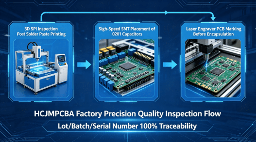
At Guangzhou Huachuang Precision Technology Co., Ltd. (HCJMPCBA), we treat stencil printing as a critical process control point. With nearly 3,500 m² of ESD‑protected manufacturing space, multiple high-speed SMT lines, and ISO9001 quality management and ISO13485 medical device quality management certifications, our 3D SPI systems verify paste volume, height, and position on every pad before components are placed — catching printing defects at the source.
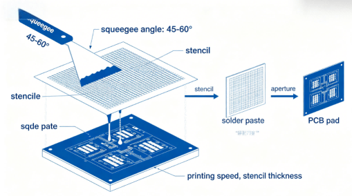
Schematic Diagram Of Stencil Printing Process
Why Stencil Printing Defects Occur
Three key factors determine printing success:
-
Stencil design and thickness — Aperture size, shape, and foil thickness directly determine paste volume
-
Printing parameters — Speed, pressure, angle, and snap-off distance must be consistent
-
Solder paste condition — Freshness, viscosity, temperature, and equipment cleanliness
When any of these variables changes, defects soon follow. Below are the six most common stencil printing defects, their root causes, and prevention strategies.
1. Inadequate or Oversize Solder Paste
Incorrect paste volume is one of the most common stencil printing issues. Insufficient paste leads to poor or defective solder joints, while excess paste makes bridging and contamination more likely.
Causes:
-
Wrong aperture size or stencil thickness
-
Inappropriate squeegee pressure
-
High solder paste viscosity or expired material
-
Poor paste release due to blocked apertures
Prevention:
-
Optimize aperture design — typically reduce by 10–20% for fine-pitch components
-
Maintain consistent squeegee pressure and printing speed
-
Store solder paste under optimal conditions and allow temperature stabilization before use
-
Implement regular stencil cleaning to prevent aperture obstruction
Consistent paste volume is the foundation of reliable solder joints. Our 3D SPI systems measure paste height, area, and calculated volume for every deposit, providing real-time Cpk data to detect volume deviations before they reach reflow.
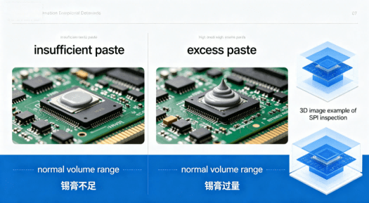
Comparison Chart Of Abnormal Solder Paste Volume
2. Solder Bridging
Solder bridges occur when adjacent pads accidentally come into contact with excess solder, resulting in electrical shorts after reflow. Bridging is particularly problematic in high-density assemblies.
Causes:
-
Excessive solder paste deposition
-
Stencil alignment error relative to PCB pads
-
Over-printing pressure pushing paste under the stencil
-
Non-uniform paste layers on the board
Prevention:
-
Use fiducial-based vision systems for accurate stencil alignment
-
Apply narrower apertures for fine-pitch devices
-
Optimize squeegee pressure to avoid paste bleed
-
Monitor volume consistency using SPI systems
Bridging must be managed at the printing stage — reflow cannot correct excess paste.
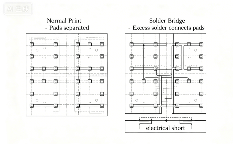
Solder Bridge Formation Schematic Diagram
3. Cold or Weak Solder Joints
Cold solder joints occur when solder fails to properly wet pads or component leads, leading to unreliable electrical connections. Although visibly identified after reflow, many cold joints originate from printing problems.
Causes:
-
Insufficient or uneven paste deposition
-
Contaminated pads or corroded components
-
Poor reflow thermal characteristics and inconsistent paste volume
Prevention:
-
Calibrate printers for uniform paste deposits
-
Confirm solder paste freshness and proper handling
-
Optimize reflow temperature profiles
-
Verify component placement prior to reflow
Stable paste deposits enable uniform solder melting and flow during heating.
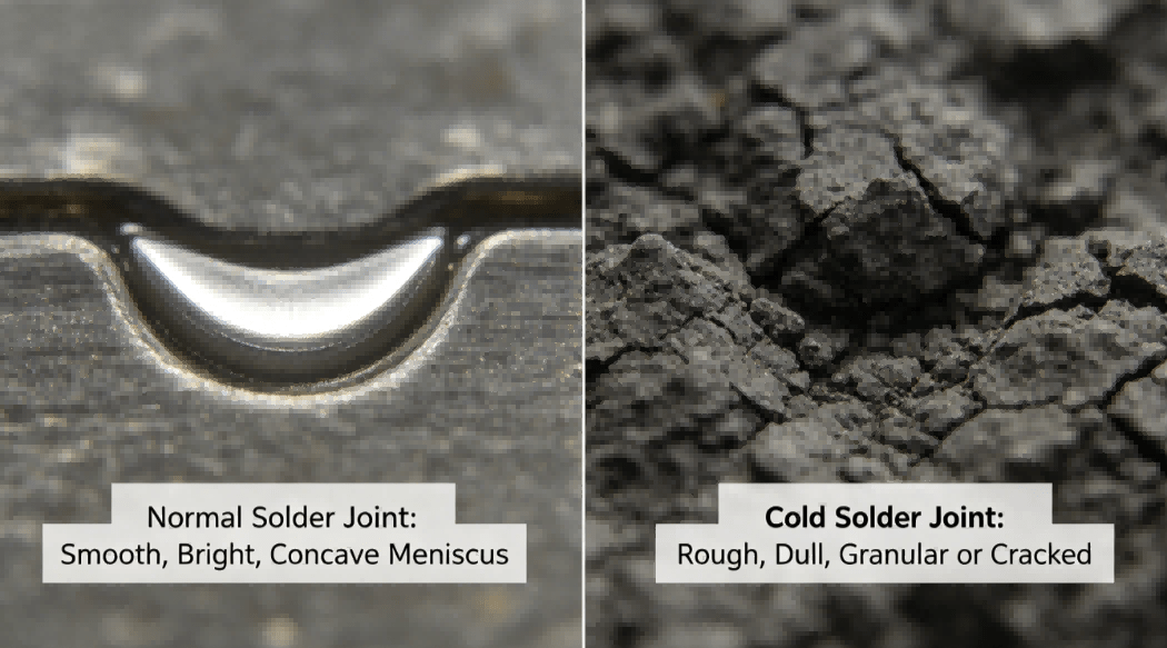
Comparison Of Cold Solder Joints Vs Normal Solder Joints
4. Tombstoning
Tombstoning occurs when small passive components stand on one pad and lift vertically during reflow, leaving the other pad disconnected. While tombstoning appears during reflow, its origin is frequently inaccurate stencil printing.
Causes:
-
Different amounts of solder paste between component pads
-
Asymmetrical pad or aperture design
-
Irregular heating during reflow
Prevention:
-
Maintain consistent paste deposition on both pads
-
Apply symmetrical stencil aperture designs
-
Ensure proper positioning and thermal profiles
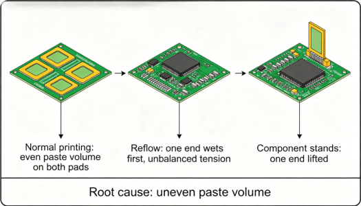
Uneven Paste Volume
5. Paste Smearing or Spillage
Smearing is the dispersion of solder paste beyond the target pad areas, contaminating adjacent pads and creating short-circuit risk.
Causes:
-
Poor stencil-to-PCB contact
-
Excessive squeegee speed or pressure
-
Residual paste on stencil underside
-
PCB flexing due to inadequate support
Prevention:
-
Use proper board support tooling to keep the PCB flat
-
Reduce printing speed for controlled paste rolling
-
Implement automatic under-stencil cleaning cycles
-
Minimize snap-off distance in contact printing
-
Clean stencil and PCB completely before direct deposits
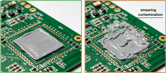
Solder Paste Smearing Contamination
6. Streaking or Stencil Drag
Stencil drag presents as streaks or irregular solder paste lines on the PCB surface.
Causes:
-
Incorrect squeegee angle or damaged blades
-
Over-pressure during printing
-
Dry or contaminated stencil surfaces
Prevention:
-
Maintain squeegee angle at 45° to 60°
-
Replace worn blades regularly
-
Increase stencil cleaning frequency
-
Ensure smooth paste rolling during printing
Early visual inspection helps detect streaking before defects propagate downstream.
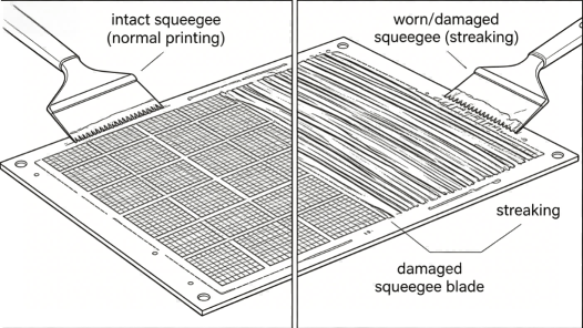
Squeegee Streaking Schematic
Best Practices for Process Control and Troubleshooting
When stencil printing defects are detected, a systematic method can quickly identify root causes:
-
Check paste deposits first — then examine placement and reflow
-
Inspect the stencil — cleanliness, flatness, and aperture condition
-
Review printing parameters — identify recent changes
-
Check solder paste records — storage conditions and viscosity
-
Use SPI data trends — analyze failure patterns
Process control is far more effective than defect correction after assembly.
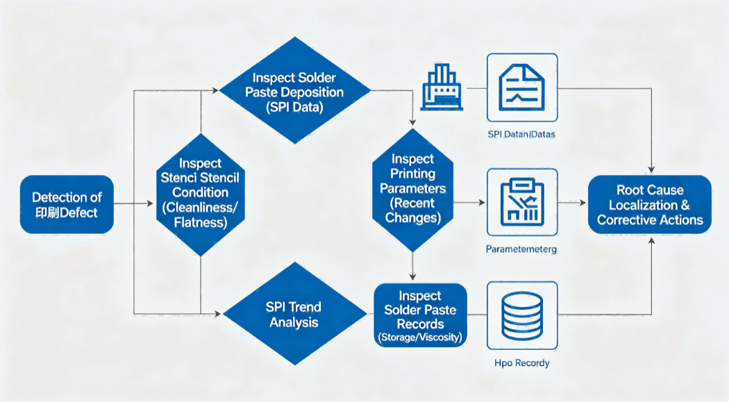
Defect Root Cause Analysis Process
Stencil Printing Defect Prevention
High-yield PCB assembly depends on disciplined process control:
-
Use high-quality laser-cut stencils
-
Lock and standardize validated printer settings
-
Wipe stencils after 5–10 prints on thick boards
-
Conduct pre-mass-production inspections
-
Maintain correct environmental conditions (temperature and humidity)
-
Review pad geometry and spacing to eliminate printing issues during design
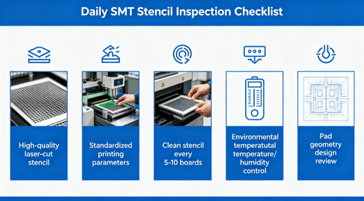
Stencil Printing Preventive Measures Checklist
HCJMPCBA: Printing Quality Built Into the Process
Successful PCB assembly starts with stencil printing. Poor solder deposition, bridging, cold joints, tombstoning, smearing, and stencil drag are all caused by variations in stencil design, printing parameters, or material handling. Our approach eliminates these variations at the source.
At Guangzhou Huachuang Precision Technology Co., Ltd. (HCJMPCBA), our printing process controls include:
-
3D SPI on every board — Paste height, area, and volume verified before component placement
-
Closed-loop feedback — SPI data automatically adjusts printer parameters for the next board
-
Laser-cut stencils — Precision apertures with consistent geometry
-
Automatic under-stencil cleaning — Prevents aperture blockage and paste contamination
-
Controlled environment — Temperature and humidity monitoring for paste stability
-
Full traceability — Every print parameter and SPI measurement logged via MES
Our nearly 3,500 m² ESD‑protected facility, multiple high-speed SMT lines, and ISO9001 and ISO13485 certifications provide the foundation for consistent, high-quality printing from prototype to volume production.
Guangzhou Huachuang Precision Technology Co., Ltd. (HCJMPCBA) — Precision stencil printing for reliable SMT assembly.