ISO 13485-Certified PCBA Processing: How Guangzhou Huachuang Precision Ensures High-Reliability for Medical, AI, and Industrial Electronics
Guangzhou Huachuang Precision Technology Co., Ltd. excels in PCBA processing. It starts with order a

This guide is maintained by the HCJMPCBA engineering team and updated with production checklists. A pcb (printed circuit board) is a non-conductive substrate featuring etched copper traces that mechanically support and electrically connect electronic components. It serves as the foundation for nearly all modern electronics, transforming raw schematics into functional hardware assemblies (pcba).
Core Definition: Understanding what a pcb circuit board is, what it stands for, and its structural anatomy (Substrate, Copper, Solder Mask, Silkscreen).
Selection Logic: How to evaluate different types of pcb (Single-Sided, Double-Sided, Multilayer, Rigid-Flex, High-Density Interconnect) based on application demands, thermal envelope, and signal speeds.
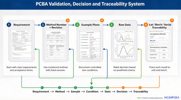
Manufacturing Quality Gate: Why volume production requires strict process controls, including Method Number + Revision tracking, IPC-A-600 standards, and full lot/batch/serial traceability.
When engineering teams discuss electronic design, the terminology can vary. What does pcb stand for in electronics? PCB stands for Printed Circuit Board. Historically referred to as a printed wiring board (PWB), the modern pcb definition encompasses both the physical mechanical structure and the electrical interconnection pathways.
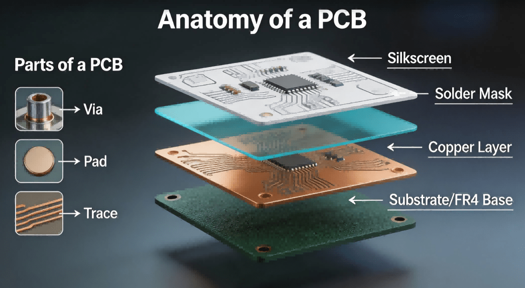
To understand what is a pcb board, it helps to examine its structural layers:
Substrate (Base Material): The core mechanical chassis, typically made of fiberglass-reinforced epoxy resin (FR-4). It provides dielectric insulation and mechanical rigidity.
Copper Foil (Conductor): Laminate layers of thin copper foil etched to form traces, pads, and planes. Copper weight usually ranges from $0.5\text{ oz}$ to $3\text{ oz/ft}^2$.
Solder Mask: A protective polymer coating (commonly green, blue, black, or white) applied over copper traces to prevent oxidation, bridge formations, and unintended short circuits during assembly.
Silkscreen (Legend): Epoxied ink printed on top of the solder mask to display reference designators, test points, component outlines, and logos.
Anatomy Of A Pcb Hcjmpcba
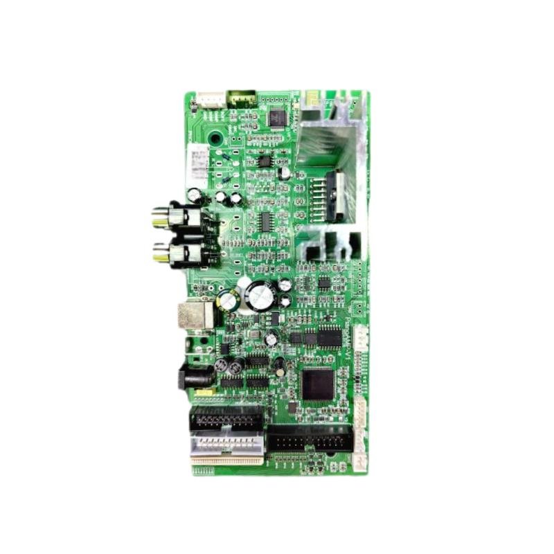
Understanding what are circuit boards made of helps differentiate a bare pcb board from a pcba circuit board. While the bare board provides structural and electrical routing, the pcba (Printed Circuit Board Assembly) represents the completed hardware populated with surface-mount devices (SMD) and through-hole components.
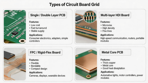
Selecting the correct board architecture requires balancing cost, space constraints, and electrical performance. Below are the primary kinds of pcb deployed in commercial and industrial hardware:
Single-sided boards feature copper on a single layer, ideal for low-density consumer electronics. Double-sided boards utilize plated through-holes (PTH) to interconnect traces across top and bottom layers, forming the backbone of standard industrial controls.
Multilayer boards stack four or more conductor layers separated by insulating prepreg and core materials. Layer counts typically range from 4 to 32+ layers in high-performance hardware, enabling dense power distributions and controlled impedance signal routing.
Rigid boards maintain shape under mechanical stress. Flexible PCBs (FPC) use polyimide substrates to bend within tight enclosures. Rigid-flex boards integrate flexible polyimide layers between rigid FR-4 sections, eliminating mechanical wire harnesses and connectors.
HDI boards utilize microvias, laser drilling, and fine trace/space geometries ($\le 75\,\mu\text{m}$) to maximize component density. They are essential for advanced microprocessors, BGA packages with tight pitch ($\le 0.4\text{ mm}$), and compact mobile hardware.
What kind of circuit boards are found in motorcycles and automotive systems? These environments subject electronics to constant vibration, wide thermal swings ($-40^\circ\text{C}$ to $+125^\circ\text{C}$), and moisture. Automotive applications rely heavily on heavy copper PCBs, High-Tg FR-4, or Metal Core PCBs (MCPCB) to handle high current loads and efficient heat dissipation.
Types Of Circuit Board Grid Hcjmpcba
| Board Type | Layer Count | Key Material / Feature | Primary Advantage | DFM Complexity |
| Single / Double-Sided | 1 – 2 Layers | Standard FR-4 / HASL | Low cost, rapid turnaround | Low |
| Standard Multilayer | 4 – 8 Layers | High-Tg FR-4 / ENIG | Balanced signal integrity & density | Medium |
| High-Layer Count | 10 – 32+ Layers | Low-Loss Epoxy / Polyimide | High signal speeds, power isolation | High |
| Rigid-Flex | 4 – 12 Layers | FR-4 + Polyimide Core | Replaces wiring harnesses, ultra-compact | High |
| Metal Core (MCPCB) | 1 – 2 Layers | Aluminum / Copper Base | Superior thermal management | Medium |
Transforming a circuit design into a scalable, high-yield product involves five structured engineering stages:
Design Output & File Generation: Export CAD data to standard manufacturing formats such as Gerber RS-274X, ODB++, or IPC-2581, along with drill tables and IPC netlists.
DFM & DFA Engineering Review: Perform Design for Manufacturability and Design for Assembly checks. Verify trace-to-space ratios, drill aspect ratios, annular rings, and thermal relief pads to prevent manufacturing defects.
Substrate Fabrication & Surface Finish: Process core laminates through photolithography, etching, lamination, and plating. Apply surface finishes like Electroless Nickel Immersion Gold (ENIG) or Organic Solderability Preservatives (OSP) based on component pitch.
Bare Board Testing: Validate electrical continuity and isolation across 100% of production boards using flying probe or dedicated bed-of-nails fixture testing per IPC-9252 standards.
PCBA Assembly & Testing: Apply solder paste, perform high-speed SMT placement, execute reflow soldering, and conduct automated optical inspection (AOI) alongside functional circuit testing (FCT).
| Inspection Parameter | Reference Standard | Inspection / Verification Method | HCJMPCBA Quality Target |
| Visual & Workmanship | IPC-A-600 Class 2/3 | Visual inspection, 180x Optical Microscope | Zero solder mask encroachment on SMT pads |
| Plating Thickness | IPC-6012 Section 3.6 | X-Ray Fluorescence (XRF) | Copper hole wall thickness $\ge 20\,\mu\text{m}$ |
| Solderability | J-STD-003 | Edge dip test, Wetting balance analyzer | $> 95\%$ wetting coverage |
| Internal Integrity | IPC-TM-650 2.1.1 | Micro-sectioning (Cross-section analysis) | Zero delamination, zero inner-layer separation |
| Cleanliness | IPC-TM-650 2.3.25 | Resistivity of Solvent Extract (ROSE) testing | $< 1.56\,\mu\text{g/cm}^2\text{ NaCl}$ equivalent |
To minimize risks for global OEM buyers and engineering teams, HCJMPCBA implements rigorous production controls across every fabrication and assembly step:
Method Number + Revision Control: Every customer project is assigned an internal engineering Method Number linked to a explicit revision state. Any engineering change order (ECO) triggers a mandatory BOM and Gerber re-validation before production release.
Sample Plan & Test Conditions: Production lots adhere to ANSI/ASQ Z1.4 sampling plans. Solderability, thermal stress, and ionic cleanliness tests are performed under defined lab conditions ($23^\circ\text{C} \pm 2^\circ\text{C}$, $50\% \pm 10\%\text{ RH}$).
Raw Data Verification: We do not rely solely on vendor certificates. Our quality team verifies raw copper thickness, laminate $T_g$ values via Differential Scanning Calorimetry (DSC), and impedance test logs using Time-Domain Reflectometry (TDR).
Full Traceability (Lot / Batch / Serial): Every production run is tracked back to the raw substrate batch, solder paste lot number, and component reel data. Individual boards can be laser-marked with 2D DataMatrix serial codes for full lifecycle traceability.
When submitting RFQs to PCB/PCBA manufacturers, engineers and buyers can insert the following quality clause directly into their project documentation:
“The supplier shall manufacture all printed circuit boards in accordance with IPC-6012 Class 2 (or Class 3 as specified) and assemble components per IPC-A-610 Class 2/3. All bare boards must undergo 100% electrical testing per IPC-9252. The supplier must maintain full raw material lot traceability (substrate, copper, solder paste) and provide a Certificate of Conformance (CoC), micro-section analysis report, and impedance test data upon delivery.”
Ignoring Z-Axis CTE in Multilayer Stackups: Selecting standard FR-4 with a high Coefficient of Thermal Expansion (CTE) in the Z-axis can lead to PTH barrel cracking during lead-free reflow profile cycles.
Specifying HASL for Fine-Pitch BGA Components: Hot Air Solder Leveling (HASL) leaves an uneven surface profile, causing solder bridging or non-wetting on BGAs or 0201/01005 components. ENIG or OSP is recommended.
Omitting Explicit Impedance Trace Specifications: Assuming a board house will automatically calculate trace widths for $50\,\Omega$ single-ended or $100\,\Omega$ differential signals without providing exact target layer stackup guidelines.
Overlooking Panel Edge Clearances for SMT Assembly: Placing components too close to the board edge ($\le 1.5\text{ mm}$) without adding breakaway tabs or V-score clearance leads to component damage during depanelization.
Selecting Suppliers Based Solely on Bare-Board Price: Focusing exclusively on initial PCB fabrication cost while ignoring assembly yields, testing capabilities, and component sourcing traceability, resulting in high scrap rates at the PCBA stage.
Consider a industrial power control device operating inside an outdoor enclosure. During early prototyping, standard mid-Tg FR-4 ($T_g 150^\circ\text{C}$) boards passed bench testing at ambient temperatures. However, during field deployment, ambient thermal cycles combined with internal MOSFET power dissipation pushed internal temperatures above $130^\circ\text{C}$.
The resulting thermal expansion caused micro-cracking in plated through-holes and subtle signal degradation. Transitioning the design to a High-Tg substrate ($T_g \ge 170^\circ\text{C}$) with a lower Z-axis expansion rate, alongside introducing a thermal copper plane connected to an aluminum heatsink enclosure, resolved the field failures. Identifying environmental operational limits early prevents costly warranty recalls.
Q1: What is a pcb board and what is its main function?
A pcb board is an insulated board with conductive copper pathways. Its primary function is to mechanically hold electronic components in place while electrically connecting them to form a working circuit.
Q2: What does pcb mean in electronics compared to pcba?
In electronics, PCB refers to the bare, unpopulated printed circuit board. PCBA stands for Printed Circuit Board Assembly, which is the complete board after all electronic components have been soldered onto it.
Q3: What are the primary parts of a pcb?
The primary parts include the dielectric substrate, copper traces/pads, solder mask, silkscreen, through-hole vias, and surface-mount pads where components are mounted.
Q4: What are the most common kinds of pcb used in consumer devices vs. industrial electronics?
Consumer devices often use double-sided, multilayer FR-4, or flexible PCBs to save space. Industrial electronics rely on heavy copper PCBs, High-Tg laminates, or metal core boards built for high reliability and heat resistance.
Q5: What is the standard thickness of an electronic printed circuit board?
The industry standard nominal thickness for a rigid electronic printed circuit board is $1.6\text{ mm}$ (approx. $0.062\text{ inches}$). Other common thicknesses include $0.8\text{ mm}$, $1.0\text{ mm}$, and $2.0\text{ mm}$.
Q6: How does a multilayer pcb printed circuit differ from a double-sided board?
A double-sided board has conductive copper only on its top and bottom surfaces. A multilayer board contains additional copper layers embedded between insulating dielectric cores inside the board, enabling complex, high-density routing.
Q7: What does pcb hardware quality depend on during volume production?
Quality depends on substrate thermal properties, copper plating consistency in via holes, precise solder mask application, rigorous DFM checks, and adherence to IPC-A-600/IPC-A-610 standards.
Q8: Why is DFM review essential before ordering a circuit pcb board?
A DFM review identifies potential design flaws—such as insufficient clearance, acid traps, or undersized pads—before manufacturing begins, preventing production delays and yield loss.
To ensure your manufacturing partner adheres to strict quality controls, you can request the following deliverables with your order:
Certificate of Conformance (CoC): Verifying material compliance with project specifications.
Micro-Sectioning Report: Cross-sectional images validating hole wall copper plating thickness and layer registration.
Impedance Test Report: TDR measurement logs confirming controlled impedance traces match tolerances ($\pm 10\%$).
Ionic Cleanliness Certificate: ROSE test data showing acceptable contamination limits.
Material Safety & Compliance Docs: RoHS, REACH, and UL94-V0 flammability certifications.
Update triggers: standard revision changes / recurring questions / production checklist updates.
Guangzhou Huachuang Precision Technology Co., Ltd. excels in PCBA processing. It starts with order a
Guangzhou Huachuang Precision Technology specializes in high-reliability BGA assembly, offering prec

Understand the core manufacturing processes and component composition of circuit card assembly (PCBA