
HCJMPCBA’s 10-Step Essential Guide: What Is a Circuit Diagram & How to Read and Design PCB Schematics for Excellence
Discover what a circuit diagram is and how to read or design a clear pcb schematic step-by-step. Und
This comprehensive industrial manufacturing guide is maintained by the HCJMPCBA engineering team and is continuously updated with production checklists. It details what are printed circuit boards made of, traces the physical manufacturing journey from a blank pcb and parts to scalable PCBA, and explains the precise process controls required to optimize production yields and eliminate field failures.
Material Chemistry Dictates Yield: Selecting the right types of pcb materials—specifically managing the Glass Transition Temperature ($Tg$) and Decomposition Temperature ($Td$)—directly prevents laminate delamination during high-temperature lead-free reflow.
Traceability Over Audits: High-reliability sectors require component and board-level traceability (lot/batch/serial) data to mitigate supply chain risks and counterfeit hardware penetration.
DFM Checks Prevent EQs: Resolving trace capacity issues and routing constraints during the design phase eliminates costly Engineering Queries (EQs) when moving from NPI prototyping to high-volume manufacturing.
| Material Classification | Core Component Combination | Thermal Rating (Tg / Td) | High-Frequency Performance (Dk / Df @ 10GHz) | Primary Industrial Use Case | SMT Mass Production Vulnerability |
| Standard FR4 | Woven Fiberglass + Epoxy Resin | $130^\circ\text{C}$ to $140^\circ\text{C}$ / $300^\circ\text{C}$ | 4.2 to 4.5 / 0.02 | General consumer electronics, basic hardware pcb, toys. | High risk of pad lifting and copper warping during multiple reflow cycles. |
| High-Tg FR4 | Modified Epoxy + Enhanced pcb fiber | $170^\circ\text{C}$ to $180^\circ\text{C}$ / $340^\circ\text{C}$ | 4.1 to 4.3 / 0.015 | Industrial control units, multi-layer electronics pcb, automotive electronics. | Hydroscopic properties; requires monitored baking conditions to avoid blistering. |
| Halogen-Free FR4 | Phosphorus/Nitrogen Resin Matrix | $150^\circ\text{C}$ to $170^\circ\text{C}$ / $330^\circ\text{C}$ | 4.0 to 4.2 / 0.012 | Green compliance electronics, telecommunication networks. | Material is inherently more brittle; requires adjusted CNC v-scoring and routing depth profiles. |
| PTCE / Rogers | Ceramic-Filled PTFE Matrix | $280^\circ\text{C}$ / $400^\circ\text{C}$ | 2.2 to 3.5 / 0.001 to 0.003 | RF, Microwave, Aerospace radar, AI server antenna arrays. | Extremely low mechanical adhesion; demands custom chemical plasma desmear pre-treatment. |
| Polyimide (PI) | Flexible Polyimide Film Layer | N/A / $600^\circ\text{C}$ | 3.2 to 3.5 / 0.008 | Rigid-flex applications, aerospace hardware, medical probes. | High moisture absorption; demands precise dwell times and dedicated fixtures in the SMT oven. |
To understand what is a pcb circuit board and how it functions under extreme industrial workloads, one must look closely at its physical and chemical construction. A finished board is a multi-layered composite sandwich engineered to provide mechanical support and reliable electrical connections.
At the absolute center of almost every standard circuit board pcb sits the pcb substrate, which provides mechanical rigidity and insulation. The most prominent printed circuit board material is FR4 (Flame Retardant 4). This circuit board fr4 composition consists of a woven pcb fiber (fiberglass) cloth thoroughly impregnated with an epoxy resin binder that meets UL94V-0 safety standards.
For applications requiring flexible routing or multi-layer integration into confined mechanical enclosures, engineers utilize different types of pcb options, such as flexible or rigid-flex configurations utilizing Polyimide films.
Conductive pathways are created using a high-purity copper circuit board layer that is thermally bonded onto the substrate. The thickness of this copper layer is typically measured in ounces per square foot (e.g., 1 oz copper equates to roughly 35 micrometers).
High-power industrial controllers demand thick copper options to handle heavy current loads without encountering excessive trace heating.
The characteristic color of a finished board pcb comes from the solder mask—a protective polymer coating applied over the copper traces. Its primary role is to insulate the copper pathways from accidental cross-bridging during automated assembly.
Exposed copper pads where parts will be soldered require an engineered surface finish, such as HASL (Hot Air Solder Leveling), ENIG (Electroless Nickel Immersion Gold), or OSP (Organic Sphericity Preservatives), to prevent oxidation and ensure stable long-term solderability.
🔍 Industrial Diagram Suggestion for WordPress:
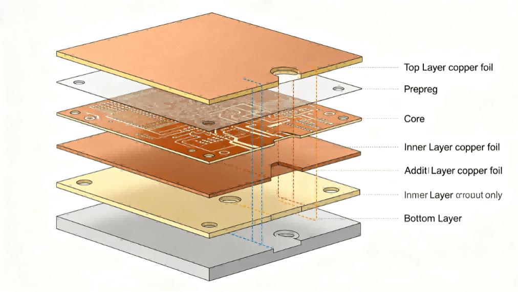
Insert a high-resolution, annotated cross-sectional 3D graphic illustrating a 4-layer PCB stack-up. Label the distinct layers clearly from top to bottom: Top Solder Mask, Top Copper Layer (Signal), Prepreg (Insulating Bond), Inner Copper Layer 1 (Ground Plane), FR4 Core Substrate, Inner Copper Layer 2 (Power Plane), Core Prepreg, Bottom Copper Layer (Signal), and Bottom Solder Mask.
Exploded View Of Laminated Structure For Hcjmpcba Multi Layer Pcb Board
When preparing a design for mass production, engineers often ask critical questions regarding trace routing and electrical continuity:
For instance, must every single VCC 3.3V node on a board be wired in a continuous sequence? The answer is: electrically yes, but physically absolutely not. While all 3.3V points must share the same final electrical potential, routing them in a single, continuous series loop (known as a daisy-chain topology) introduces massive voltage drops (IR Drop) and significant parasitic inductance. This causes components at the end of the chain to malfunction due to inadequate voltage.
Furthermore, mixing digital and analog supply lines creates severe signal degradation. High-speed digital switching generates massive high-frequency noise. If a sensitive analog sensor node shares a direct, unmanaged 3.3V physical trace with a digital micro-controller, that digital noise will pollute the analog measurements.
The correct production method is to employ a Star Topology. In this configuration, separate, isolated power branches run directly from the main power management IC out to individual sub-circuits. These independent branches are isolated at the source using ferrite beads or 0-ohm resistors, guaranteeing stable power distribution without noise cross-contamination.
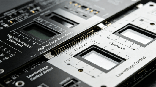
Why do professional boards incorporate physical and electrical isolation zones? Circuit isolation is an absolute requirement for safety, equipment protection, and noise management:
High-Voltage Safety: In industrial motor drives or power converters, an isolation barrier separates the dangerous high-voltage AC section (e.g., 220V/400V) from the safe, low-voltage control logic (3.3V/5V). This prevents a component breakdown on the power side from sending catastrophic voltages through the control circuit, protecting both the hardware and human operators.
Eliminating Ground Loops: When different sub-modules operate across a large system, minor variations in ground resistance cause ground loop currents to flow through signal wires. This injects severe low-frequency hum and data corruption. Physical isolation breaks this loop, allowing clean data transmission via optocouplers or digital isolators.
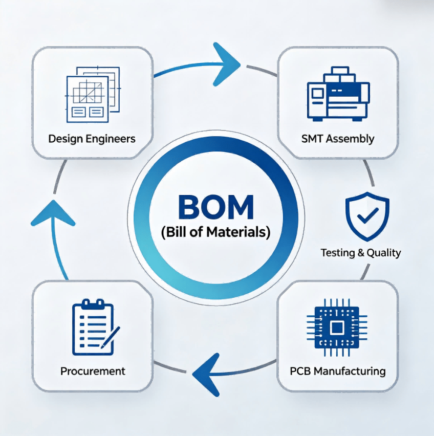
Transitioning from a digital design to a physically assembled, high-volume printed circuit materials product is a highly automated process. Each stage must be controlled using specific engineering protocols to achieve zero-defect yields.
Before production begins, manufacturing data is locked using a specific Method Number + Revision tracking system. This step ensures that any modifications made during the Design for Manufacturability (DFM) check are saved under a strict revision history, eliminating the risk of running outdated schematic versions on the line.
Raw printed circuit board laminate sheets are cut to panel sizes. For high-reliability boards, the material must match strict factory test conditions (such as IPC-4101E compliance checking for resin content and dimensional stability under heat).
A photosensitive film is applied to the copper-clad pcb substrate. UV light projects the circuit patterns onto the panel. Unwanted copper is chemically etched away, leaving pristine, high-definition trace networks.
Before multi-layer lamination occurs, 3D AOI systems inspect the inner traces against the original design files. Any microscopic trace thinning or residual copper bridging is caught and rejected immediately.
The etched inner layers, raw insulating prepreg sheets, and outer copper foil sheets are stacked under extreme heat and pressure. This fuses the components into a single, cohesive pcb board layers matrix.
Advanced CNC drilling machines create via holes through the board stack-up to connect different layers. For high-density layouts, laser drilling is utilized to create blind and buried micro-vias.
🔍 Industrial Diagram Suggestion for WordPress:
Place a dual-panel photo graphic here. The left side should show an automated CNC high-speed drilling spindle working on an array of production panels. The right side should display a real-time, high-contrast 3D SPI (Solder Paste Inspection) color-coded height analysis screen, illustrating precise, consistent deposition across microscopic BGA pads.
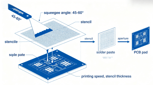
Once the bare board fabrication is complete, it enters the PCBA assembly line. A high-precision stencil prints lead-free solder paste onto the component pads.
Every single panel undergoes a mandatory 3D SPI scan. The system measures paste volume, height, and registration alignment. This Sample Plan adheres to zero-acceptance-defect standards; if even a single pad displays insufficient volume, the entire panel is automatically rejected before reaching the component mounters, preventing hidden open-joint or cold-solder defects.
Hcjmpcba Pcb Industrial Control Board With Physical Slotting
To ensure the integrity of high-volume electronics manufacturing, buyers should demand objective, data-driven validation metrics at every checkpoint.
[Raw Material Entry] ---> [3D SPI Scan] ---> [Reflow Oven] ---> [3D AOI & X-Ray] ---> [Functional FCT]
        |                    |                     |                  |                    |
  (IPC-4101E Check)    (Volume Gate)        (Profile Test)     (Voiding Analytics)   (Raw Data Report)
| Manufacturing Validation Stage | Factory Inspection Protocol | Operational Test Conditions | Deliverable Quality Evidence |
| Incoming Material Integrity | IPC-4101E Material Verification | Thermal Stress Testing: 3 cycles at $288^\circ\text{C}$ for 10s. | Material Certificate & Delamination Resistance Report |
| Solder Deposition Precision | 100% Inline 3D Solder Paste Inspection (SPI) | Volumetric thresholds locked to 80%–120% of theoretical stencil volume. | Automated SPC Real-Time CPK Charts |
| Structural Solder Integrity | 100% Post-Reflow 3D AOI + Transmission X-Ray | BGA/QFN voiding ratio analyzed; maximum allowable threshold capped at < 15% total area. | High-Resolution X-Ray Radiographs & Defect Logs |
| Parametric Electrical Function | Customized Automated Functional Testing (FCT) | Full-cycle voltage/current sweeping, signal integrity monitoring under simulated loads. | Full Electronic Raw Data Parametric Logs |
| System-Level Traceability | Laser-Etched 2D DataMatrix Tracking | Serialized verification scanned automatically at each conveyor station. | Comprehensive Traceability (lot/batch/serial) Manifest |
Global procurement managers can copy and paste this standard requirements clause directly into their Request for Quotation (RFQ) documentation to enforce strict manufacturing compliance:
Section 7.4 – Electronic Manufacturing Service Quality Deliverables Clause:
The contract electronics manufacturing service provider (EMS) must execute all production lots under an active IATF 16949 / ISO 9001 quality framework. The manufacturer is required to supply a complete production documentation package upon project completion. This package must include:
Complete engineering drawing sign-offs indicating the unique Method Number + Revision.
Full-spectrum 3D AOI and transmission X-Ray voiding analysis Raw Data logs.
Verified Traceability (lot/batch/serial) reports tracking every primary IC back to its original authorized distributor component lot code.
Any deviations from these standards will result in immediate lot rejection.
Hcjmpcba High Precision Multi Layer Board Vacuum Lamination Press
Metric vs. Imperial Footprint Confusion: Mixing up imperial 0603 components with metric 0603 footprints (which match imperial 0201 packages) causes massive layout mismatches that halt automated placement lines.
Mismatched Thermal Expansion Coefficients ($CTE$): Pairing standard low-$Tg$ FR4 cores with high-layer-count configurations leads to extreme vertical expansion during lead-free wave soldering, tearing apart internal via connections.
Omitting Thermal Relief Pads on Large Copper Planes: Connecting component pads directly into large power or ground copper planes without thermal relief cutouts creates a massive heat sink. This causes cold-solder joints and component warping during reflow.
Selecting OSP Surface Finish for Multi-Stage Reflow: Specifying a standard Organic Sphericity Preservative (OSP) finish for complex, double-sided boards often results in the protective film breaking down during the first oven pass, leaving opposite pads oxidized before the second SMT run.
Neglecting High-Frequency Dielectric Loss ($Df$): Using standard, economical FR4 materials for gigahertz-range RF circuits causes excessive signal attenuation and thermal dissipation issues, degrading product performance.
When introducing a New Product Introduction (NPI) design featuring fine-pitch BGA components, using traditional, unverified manufacturing workflows carries immense financial risk.
By applying strict pre-production DFM filtering, verifying material properties before assembly, and locking down tracking metrics from day one, you ensure that your initial low-volume prototypes translate seamlessly into automated high-volume runs without encountering costly layout or soldering defects.

100% Aoi Inspection During Smt Production Hcjmpcba
Q1: What are the primary differences between standard FR4 and high-frequency Rogers materials?
A: The primary differences center around the Dielectric Constant ($Dk$) and Dissipation Factor ($Df$). Standard FR4 exhibits a fluctuating $Dk$ (around 4.5) that degrades signal integrity above 1 GHz, along with a high $Df$ (around 0.02) that causes noticeable signal loss. Rogers laminates deliver an exceptionally stable $Dk$ (typically 2.2 to 3.5) and a ultra-low $Df$ (approximately 0.001), making them essential for high-frequency microwave and high-speed digital communications.
Q2: Why is the exact Manufacturer Part Number (MPN) suffix critical in the BOM?
A: The full MPN suffix specifies critical ordering parameters, such as the exact component packaging style (e.g., Tape & Reel vs. Bulk tubes), temperature tolerance ratings, and specific package pin-out options. Omitting the suffix can cause procurement teams to purchase loose components that cannot be loaded onto automated SMT feeder lines, delaying production.
Q3: How does a factory manage moisture-sensitive devices (MSDs) during assembly?
A: All incoming moisture-sensitive components are categorized based on their J-STD-033 Moisture Sensitivity Level (MSL). Components are stored in humidity-controlled dry cabinets. If exposure time limits are exceeded prior to reflow, the parts undergo a documented baking cycle to remove internal moisture, preventing internal component cracking during soldering.
Q4: What is the purpose of conducting a pre-production strip-and-etch test?
A: A strip-and-etch test is an destructive quality audit performed on a sample board from each fabrication run. The copper layers are chemically stripped away to verify actual internal trace widths, layer registration accuracy, and the thickness of the core insulation material against the original design parameters.
Q5: Why is a 3D SPI system superior to standard 2D automated visual inspection?
A: A 2D inspection system can only check the two-dimensional area coverage of printed solder paste, completely missing critical height variations. A 3D SPI system utilizes laser profile scanning to calculate the exact three-dimensional volume, height distribution, and alignment profile of the paste deposit, stopping potential defect joints before components are placed.
Before your high-volume production lot leaves our loading docks, you have the right to request the following data packages for review:
The Complete SMT Thermal Profile Report: Micro-sensor tracking logs verifying the exact preheat, liquidus time, and cooling ramp rates used for your specific assembly run.
Volumetric Micro-Voiding Radiographs: High-resolution X-Ray imaging data detailing internal solder joint structure and density validation across all hidden BGA packages.
Full Parametric Pass/Fail Testing Sheets: The raw data logs captured from our automated functional test fixtures, confirming that your boards meet all operational specifications.
Update triggers: standard revision changes / recurring questions / production checklist updates.
Discover what a circuit diagram is and how to read or design a clear pcb schematic step-by-step. Und
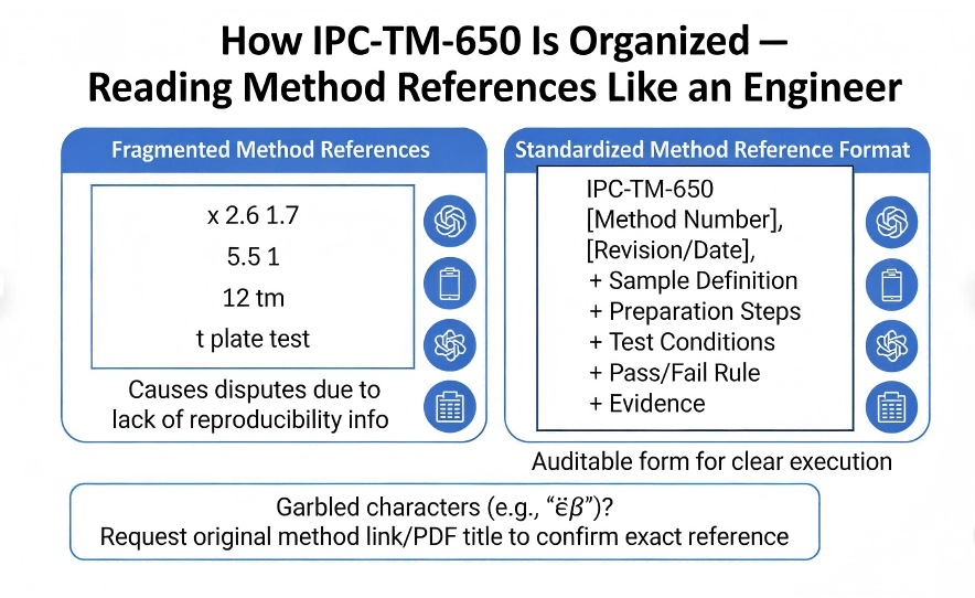
What is ipc-tm-650 and how does it help PCB and PCBA teams control quality with consistent, comparab
Guangzhou Huachuang Precision Technology Co., Ltd. (HCJMPCBA) is a leading ISO 13485-certified PCB