Mastering HCJM PCBA Manufacturing: A 10+ Key Processes Guide to End – to – End Excellence
Introduction In the realm of modern electronics manufacturing,the assembly of printed circuit boards
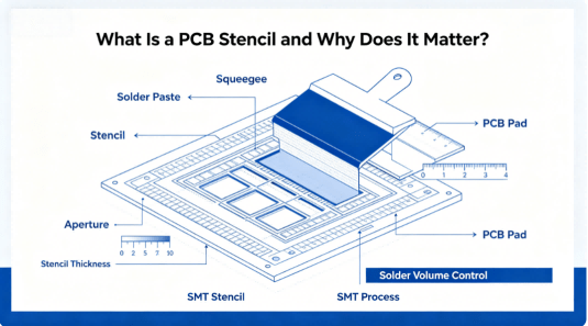
What Is A Pcb Stencil And Why Does It Matter
A PCB stencil is a precision-manufactured template used during SMT assembly to deposit a controlled volume of solder paste onto PCB pads before component placement. Whether called a solder stencil, solder paste stencil, SMT stencil, or circuit board stencil, its purpose remains the same: ensuring every solder joint receives the correct amount of solder paste.
Without a properly designed stencil, manufacturers may experience solder bridging, insufficient solder, tombstoning, solder balls, open circuits, and reduced assembly yield. For this reason, stencil design is often considered one of the most influential process-control elements in modern PCB assembly.
This guide is maintained by the HCJMPCBA engineering team and updated with production checklists, stencil validation records, SPI inspection data, and manufacturing process revisions.
1. Most SMT Defects Begin Before Reflow
Many engineers focus on pick-and-place accuracy or reflow profiles. However, numerous soldering defects originate during solder paste printing. A poor stencil design can create quality issues long before components enter the oven.
2. Stencil Design Has a Greater Impact Than Most Buyers Realize
The difference between a standard stencil and a well-engineered stencil is often measured in production yield, repair costs, and long-term field reliability rather than initial purchase price.
3. Verification Is More Important Than Thickness Alone
Choosing a 0.10 mm or 0.12 mm stencil is only one part of the equation. True process control comes from SPI verification, revision management, aperture optimization, and traceability systems.
In electronics manufacturing, a stencil is a thin sheet containing thousands of precisely laser-cut openings that correspond to solder pads on a PCB.
During production, the stencil is aligned above the PCB surface. Solder paste is then forced across the stencil using a squeegee blade. The paste fills the openings and transfers onto the pads beneath.
After stencil removal, a controlled deposit of solder paste remains on the board, ready for component placement and reflow soldering.
A PCB stencil serves the same purpose as a printing template. The difference is that modern SMT assembly requires extremely precise volume control, often measured in microns.
For advanced assemblies containing:
Even minor deviations in solder paste volume can affect reliability.
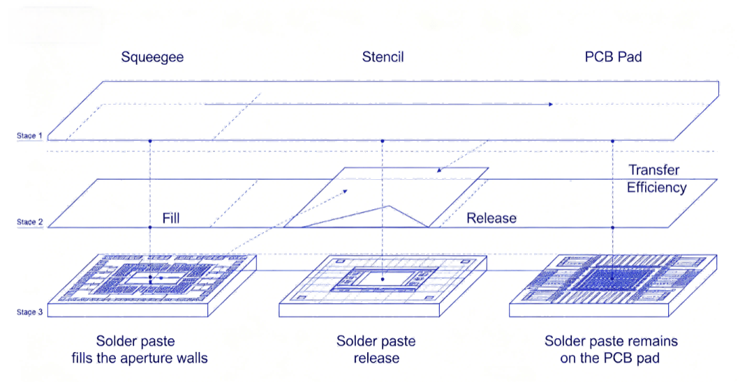
How A Pcb Stencil Transfers Solder Paste
The stencil printing process follows a simple but highly controlled sequence:
Although the sequence appears straightforward, every variable affects the outcome:
This is why experienced PCBA manufacturers treat stencil printing as an engineering discipline rather than a routine production step.
The vast majority of modern SMT production uses laser-cut stainless-steel stencils.
Advantages include:
Most industrial and commercial PCBA projects rely on stainless steel stencils because they provide consistent printing performance across thousands or even millions of print cycles.
Many high-end stencil manufacturers additionally use:
These enhancements improve solder paste transfer efficiency and reduce paste residue inside apertures.
Polyimide stencils are generally used for:
Advantages:
Limitations:
For low-volume prototyping, polyimide stencils can be practical. However, they are rarely suitable for high-reliability mass production.
A step-down stencil contains multiple thickness regions on a single stencil.
This design is often necessary when a board contains:
For example:
A robotics control board may require:
Without a step-down stencil, one component group may receive excessive solder while another receives insufficient solder.
The result can be:
Standard Stencil Vs Nano Coated Stencil
Suitable for:
Benefits:
Suitable for:
Benefits:
Most production-oriented PCBA facilities prefer framed stencils for long-term manufacturing stability.
| Application | Recommended Stencil | Risk Level | Production Volume |
|---|---|---|---|
| Prototype Development | Polyimide Stencil | Medium | Low |
| Engineering Validation | Frameless Stainless Steel | Low | Low-Mid |
| Standard Production | Framed SMT Stencil | Low | Medium-High |
| Fine-Pitch BGA Assembly | Step-Down Stencil | Lowest | Medium-High |
| Robotics & Industrial Controllers | Custom Aperture Design + Nano-Coated Stencil | Lowest | High |
The correct stencil selection depends on component density, assembly complexity, and long-term reliability requirements rather than simply choosing the cheapest available option.
One of the primary functions of a PCB stencil is controlling solder paste volume.
Hand dispensing can introduce significant variation between boards.
Stencil printing enables:
This becomes increasingly important as component size decreases.
Modern assemblies may contain:
Such devices cannot tolerate significant paste volume variation.
Yield directly affects manufacturing cost.
Even a small reduction in defects can significantly improve production efficiency.
A properly engineered stencil helps reduce:
By preventing these defects before component placement, manufacturers avoid expensive rework later in the process.
Automated assembly equipment relies on predictable solder paste deposits.
Modern pick-and-place systems assume that every pad contains the correct paste volume.
When stencil performance becomes inconsistent:
For this reason, stencil design is one of the foundational elements of automated PCB assembly.
Many engineers view a stencil as a simple consumable. In reality, the stencil is one of the most influential process-control tools in SMT manufacturing.
A well-designed stencil can improve yield, reduce rework, and increase long-term reliability. A poorly designed stencil can create defects that remain hidden until products reach the field.
The aperture is the opening through which solder paste transfers to the PCB pad.
At first glance, designing an aperture appears straightforward:
Pad size = Aperture size.
However, modern assemblies rarely follow this simple rule.
Engineers must consider:
If apertures are too large:
If apertures are too small:
This is particularly important for:
For many applications, stencil aperture design influences yield more than printer settings.
Stencil thickness determines the theoretical volume of solder paste that can be deposited.
Common industry examples include:
| Component Type | Typical Stencil Thickness |
|---|---|
| Standard SMT | 0.12 mm |
| Fine-Pitch QFN | 0.10 mm |
| Micro-BGA | 0.10 mm |
| Mixed Technology | Step-Down Design |
| Power Electronics | 0.15 mm (specific areas) |
Selecting thickness requires balancing:
The objective is not maximizing solder volume.
The objective is achieving the correct solder volume.
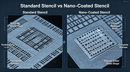
Modern stencil manufacturing increasingly uses nano-coating technologies.
Nano-coatings reduce surface energy inside stencil apertures.
Benefits include:
This is particularly beneficial when assembling:
As component density increases, paste release consistency becomes increasingly important.
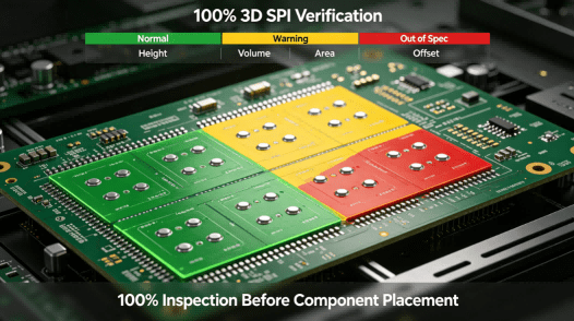
100% 3d Spi Verification
Show a cross-sectional view containing:
Highlight how solder paste fills apertures and transfers onto pads.
Suggested caption:
“Controlled solder paste deposition begins with precise stencil design.”
Microscope comparison:
Left Side:
Right Side:
Suggested caption:
“Nano-coated apertures improve solder paste transfer efficiency for high-density assemblies.”
Visualize:
Different colors can represent varying stencil thicknesses.
Suggested caption:
“Step-down stencil technology balances solder volume across mixed-component assemblies.”
Display:
Use production-style inspection screenshots.
Suggested caption:
“100% SPI verification detects solder paste defects before component placement.”
Display a PCB with a unique serial number.
Connect it visually to:
Suggested caption:
“Complete traceability links process data to every shipped assembly.”
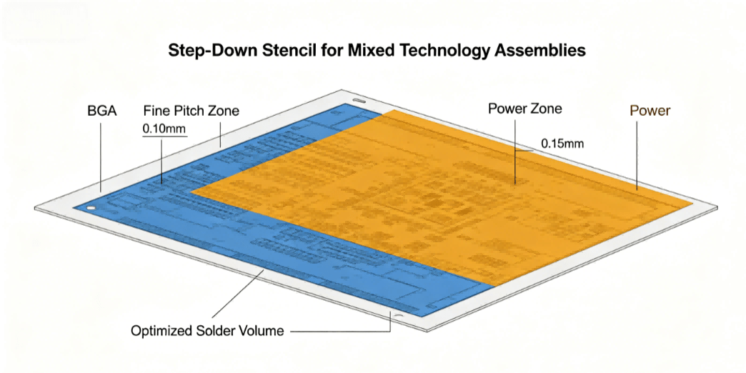
Step Down Stencil For Mixed Technology Assemblies
Engineering teams begin by analyzing:
Potential risks are identified before stencil design begins.
Stencil openings are optimized according to:
Aperture reduction or modification may be applied for:
Laser cutting creates highly accurate apertures.
Additional processes may include:
Stencil quality directly influences printing performance.
Before production:
This reduces setup variation.
The printer deposits solder paste through stencil apertures.
Critical variables include:
SPI verifies:
Defects are identified before component placement.
This is significantly less expensive than correcting defects later in production.
Only verified boards proceed to:
This creates a controlled manufacturing workflow.
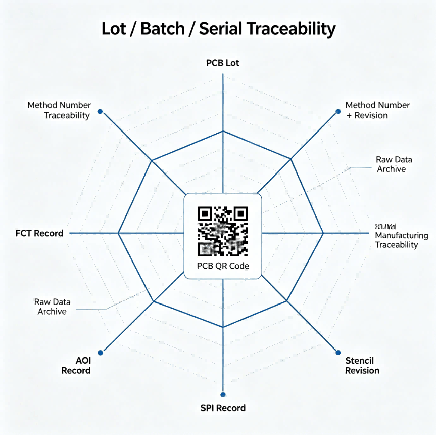
Lot Batch Serial Traceability
Modern manufacturing requires more than a stencil supplier.
It requires a documented process-control system.
Every production project receives:
Whenever stencil parameters change, revisions are recorded and validated.
This prevents undocumented process drift.
Validation activities follow structured sampling plans.
Depending on project requirements:
may be implemented.
This ensures process stability before volume production.
Critical stencil-printing parameters are documented.
Examples include:
Documented test conditions help maintain repeatability across production lots.
Rather than relying solely on pass/fail decisions, modern factories increasingly store production data.
Examples include:
Raw data provides objective evidence of process performance.
At HCJMPCBA, traceability can connect:
This structure simplifies root-cause analysis and supports long-term quality management.
| Verification Item | Industry Practice | Evidence Available |
| Stencil Thickness | Sampling | Measurement Records |
| Aperture Accuracy | Supplier Report | Incoming Verification |
| SPI Coverage | Partial Sampling | 100% Inspection |
| Process Revision | Manual Tracking | Controlled Revision System |
| Traceability | Batch-Level | Lot/Batch/Serial Tracking |
| Production Data | Pass/Fail Only | Raw Data Archive |
Mistake 1: Selecting Thickness Before Component Analysis
Stencil thickness should follow component requirements, not convenience.
Mistake 2: Ignoring QFN and BGA Aperture Optimization
Default aperture designs frequently create reliability issues.
Mistake 3: Reusing Old Stencil Designs
A PCB revision may require a stencil revision.
Ignoring this relationship introduces risk.
Mistake 4: Skipping SPI Verification
Without SPI, many defects remain invisible until later stages.
Mistake 5: No Traceability Between Stencil and Production Lot
When defects occur, root-cause analysis becomes significantly more difficult.
Consider a robotics control board containing:
Challenges include:
A step-down stencil combined with SPI verification can significantly improve process consistency.
The project may additionally benefit from:
These controls help maintain quality during transition from prototype to mass production.
Purchasing teams may directly include the following clause in RFQs, supplier qualification documents, or manufacturing agreements:
Supplier shall provide documented stencil specifications, including thickness, aperture design methodology, and revision control records.
Supplier shall maintain traceability linking PCB lot, solder paste batch, stencil revision, production date, and assembly serial number.
Supplier shall provide SPI inspection evidence, process validation records, and applicable raw production data upon request.
Any process changes affecting solder paste deposition shall be controlled through a documented Method Number and Revision system.
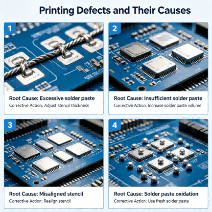
Production shall comply with applicable IPC workmanship requirements and customer-specific acceptance criteria.Top Printing Defects And Their Causes
Q1: What is the difference between a PCB stencil and a solder paste stencil?
There is no practical difference in SMT manufacturing.
Both terms generally refer to the metal template used to transfer solder paste onto PCB pads before component placement.
However, some engineers use “PCB stencil” as the broader term and “solder paste stencil” as the process-specific term.
Q2: Why can’t solder paste simply be dispensed directly onto pads?
Dispensing works well for selective applications and prototypes.
However, modern SMT production often contains:
Manual or automated dispensing cannot achieve the same throughput and consistency as stencil printing.
For high-volume PCBA production, stencil printing remains the dominant solution.
Q3: How does stencil thickness affect solder joint reliability?
Stencil thickness directly controls deposited solder volume.
Too much solder may cause:
Too little solder may cause:
The optimal thickness depends on:
The objective is controlled solder volume, not maximum solder volume.
Q4: What is a Step-Down Stencil?
A step-down stencil contains multiple thickness zones.
For example:
This allows different solder volumes to be deposited on the same board.
Step-down stencils are common in:
Q5: Why is SPI considered critical in modern SMT manufacturing?
SPI identifies defects before component placement.
Typical defects include:
Correcting defects before reflow is significantly cheaper than repairing completed assemblies.
Many advanced SMT lines now treat SPI as a mandatory quality gate.
Q6: How often should a stencil be cleaned?
The answer depends on:
Many facilities use automatic cleaning intervals based on:
The best practice is data-driven cleaning rather than fixed intervals.
Q7: What should engineers ask a PCB stencil manufacturer?
Key questions include:
These questions reveal whether the supplier is focused on precision manufacturing or simply selling commodity stencils.
Q8: Why does HCJMPCBA emphasize traceability for stencil printing?
Many soldering defects originate during paste deposition.
Without traceability, root-cause investigations become difficult.
Traceability allows engineers to link:
This improves corrective actions and long-term process stability.
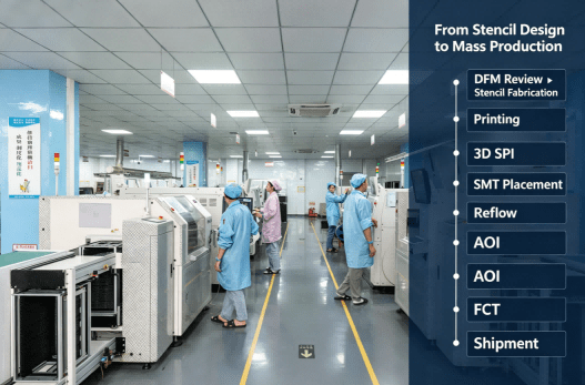
From Stencil Design To Mass Production
Many buyers focus on certifications.
Experienced engineers often focus on process evidence.
The following evidence provides stronger insight into manufacturing capability than marketing materials alone.
Request:
This confirms the stencil matches design requirements.
Request examples showing:
Raw data reveals actual process performance.
Ask suppliers to demonstrate:
Mature manufacturers maintain documented revision systems.
Request:
These documents demonstrate structured validation.
Ask suppliers to trace one finished board backward to:
Factories with strong traceability can usually perform this exercise within minutes.
Examples include:
These metrics help evaluate manufacturing consistency.
The stencil-control methodology discussed in this guide is particularly valuable for:
High-density control systems often contain:
Precise solder volume is essential.
Equipment frequently operates:
Manufacturing consistency directly affects field reliability.
Regulated products require:
Stencil process control supports compliance requirements.
Automotive assemblies face:
Robust solder joints begin with accurate solder paste deposition.
A PCB stencil is far more than a sheet of stainless steel with openings cut into it.
It is the primary mechanism controlling solder paste volume, one of the most important variables affecting SMT assembly quality.
Understanding stencil design principles—including aperture optimization, thickness selection, nano-coating technologies, SPI verification, and traceability—helps engineers reduce defects before they occur.
For purchasing teams, evaluating stencil process control is often one of the fastest ways to distinguish a mature manufacturing partner from a commodity assembler.
For manufacturing teams, the combination of:
creates a framework for repeatable and scalable production quality.
As electronics continue moving toward higher density, finer pitch components, and greater reliability expectations, stencil engineering will remain one of the foundational disciplines behind successful PCBA manufacturing.
Before approving a supplier, request:
✅ Stencil thickness verification
✅ Aperture inspection reports
✅ SPI raw data samples
✅ Method Number + Revision records
✅ Sample Plan documentation
✅ Traceability demonstration
✅ Process capability reports
✅ Production change-control procedures
Update triggers: standard revision changes / recurring questions / production checklist updates.
Introduction In the realm of modern electronics manufacturing,the assembly of printed circuit boards

Automated Optical Inspection (aoi inspection pcb) is a non-contact, high-speed quality control metho
Need to understand a 5 pin switch keyboard socket and how 3-pin vs 5-pin switches affect your keyboa