How to Use a Multimeter: The Complete Practical Guide for Engineers and Beginners
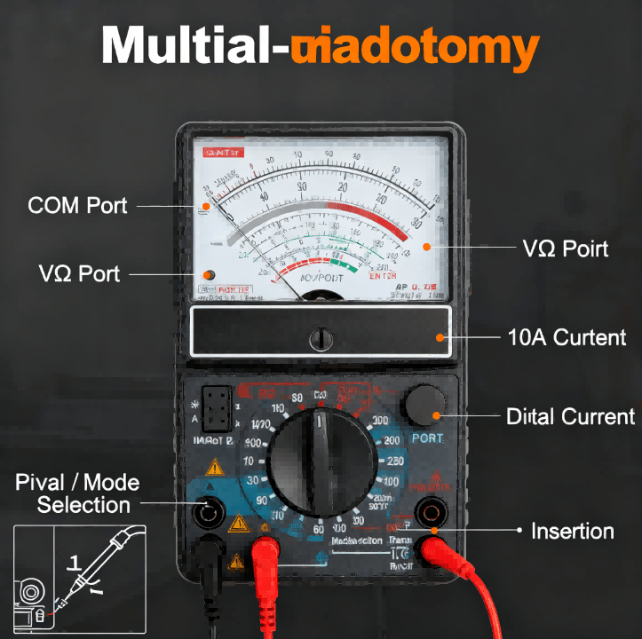
If you want to quickly understand how to use a multimeter, this guide explains the practical steps u

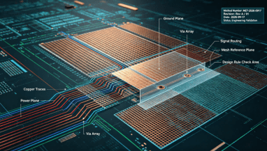
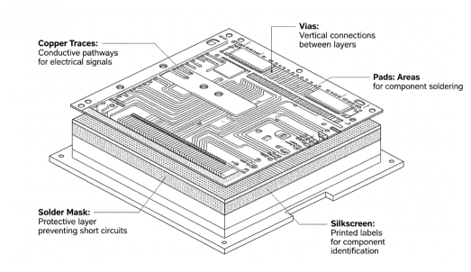
A copper trace PCB utilizes conductive copper traces (commonly referred to as electronic traces) to route electrical power and data signals across insulating circuit board substrates. Proper trace pcb design and accurate calculation using the PCB resistance formula are vital for minimizing voltage drops, preventing overheating, and ensuring signal integrity. Governed by IPC and UL standards, high-reliability copper routing serves as the backbone of modern electronics. This guide is maintained by the HCJMPCBA engineering team and updated with production checklists.
Current Capacity & Thermal Dynamics: Trace width, copper weight (thickness), and allowable temperature rise directly dictate how much current a conductor can safely carry without degrading.
Accurate Resistance Calculation: Applying the correct PCB resistance formula based on copper resistivity and dimensional geometry prevents unexpected voltage drops in power delivery networks.
Rigorous Fabrication & Testing: Combining advanced photolithography with 100% automated electrical testing eliminates hidden defects such as etching cuts, micro-cracks, and trace bridging.
Evaluating a contract manufacturer for custom printed circuit board production requires looking beyond basic fabrication quotes. The decision matrix below contrasts standard low-cost fabricators with a tier-1 precision manufacturer like HCJMPCBA.
| Evaluation Metric | Standard Low-Cost Fabricator | Tier-1 Precision Manufacturer (HCJMPCBA) |
| Engineering Review (DFM) | Basic Gerber file check; skips detailed impedance and trace width feedback. | Comprehensive DFM review, strict method number + revision tracking, and copper balancing analysis. |
| Etching Precision | Prone to over-etching, causing erratic trace widths and impedance shifts. | Advanced automated optical etching lines maintaining ultra-tight line width/space tolerances ($\pm 10\%$). |
| Testing Protocols | Random visual checks; basic open/short sampling on high-volume runs. | 100% automated electrical testing (Flying Probe / ICT) with complete raw data logging. |
| Traceability | Minimal paper logs; loose batch identification. | Full end-to-end traceability (lot/batch/serial) from raw copper laminate to final packaged boards. |
Before any design enters the production floor, our engineering team conducts a thorough review of the Gerber files, drill files, and stack-up definitions. We assign a unique method number + revision code to every engineering change order. This guarantees that layout modifications are synchronized instantly across all fabrication lines, preventing the production of obsolete board revisions.
Hcjmpcba Pcb 3d Layout
High-performance circuit boards require premium base materials, such as high-Tg FR-4 laminates and certified electrolytic copper foils. We deploy a structured sample plan that allows engineers to validate trace widths, spacing, and stack-up parameters on prototype runs before committing to large-scale volume manufacturing.
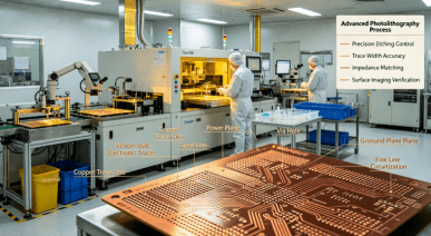
The transformation of raw copper-clad laminate into functional electronic traces relies on precision photolithography and chemical etching. Board surfaces are coated with photoresist, exposed to UV light through design phototools, and selectively etched to define exact copper traces without undercutting or copper thinning.
Hcjmpcba Smt Workshop
To ensure zero defects, inner and outer layers are scanned using Automated Optical Inspection (AOI) systems to detect potential short circuits, open traces, or etching irregularities. For high-speed boards, Time-Domain Reflectometry (TDR) testing verifies that trace impedances match design specifications.
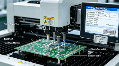
Quality assurance culminates in rigorous electrical verification. We subject finished boards to 100% electrical open/short testing under controlled test conditions (such as specified test voltages and threshold currents). We log precise raw data metrics for every tested panel to guarantee absolute reliability.
Hcjmpcba Ict
| Test Parameter | Standard / Specification | Acceptance Criteria | Provided Evidence |
| Trace Resistance & Continuity | IPC-A-600 / IPC-2221 | Zero open circuits, zero short circuits, resistance within calculated tolerance. | Automated test log report (Raw Data) |
| Impedance Control | IPC-2141 | Characteristic impedance within $\pm 10\%$ of target value (e.g., $50\,\Omega$). | TDR impedance test report |
| Etching Line Width Tolerance | IPC-A-600 Class 2/3 | Trace width and spacing maintained within design specifications. | AOI optical inspection report |
| Thermal Stress Endurance | IPC-TM-650 | No delamination, blistering, or trace cracking after solder float testing. | Thermal stress test certificate |
To streamline procurement and eliminate ambiguity in your supply chain contracts, you can directly copy and paste the following quality assurance clause into your Purchase Orders:
“The supplier shall manufacture all PCB fabrication units in strict compliance with IPC-A-600 and IPC-2221 standards. 100% automated electrical testing (open/short isolation) must be performed prior to shipment. The supplier is required to provide complete laminate lot/batch traceability records and raw electrical test data logs with every delivery.”
Ignoring Trace Temperature Rise: Failing to account for current-induced Joule heating when designing power traces leads to excessive thermal stress and board delamination.
Misapplying the PCB Resistance Formula: Neglecting copper resistivity temperature coefficients or incorrect conversion between ounces per square foot ($\text{oz/ft}^2$) and mils/micrometers results in severe voltage drop miscalculations.
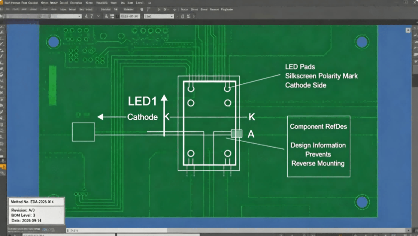
Neglecting Strict Version Control: Omitting a formal method number + revision tracking framework during layout updates results in mismatched board revisions being fabricated.
Accepting Statistical Sampling for Dense Boards: Relying on basic random batch sampling instead of 100% electrical open/short testing for high-density interconnects introduces unacceptable operational risks.
Failing to Check Minimum Trace Spacing: Setting trace-to-trace clearances below manufacturing thresholds causes etching bridging and intermittent short circuits during chemical processing.
Advanced circuit board architectures and high-density copper traces are indispensable across a wide spectrum of modern industries:
Automotive Battery Management Systems (BMS): Routing high-current paths safely while maintaining strict thermal and voltage regulation limits.
Power Electronics & Motor Drives: Managing heavy power distribution and minimizing resistive power losses across thick copper layers.
High-Frequency Telecommunications: Ensuring precise impedance matching and low-loss propagation for RF and 5G network hardware.
Industrial Automation Controllers: Delivering reliable signal routing inside vibration-prone and electrically noisy factory environments.
Q1: How do you use the PCB resistance formula to calculate trace voltage drop?
The resistance $R$ of a copper trace is calculated using the formula $R = \rho \cdot \frac{L}{A}$, where $\rho$ is the resistivity of copper, $L$ is the trace length, and $A$ is the cross-sectional area (trace width $\times$ thickness). Multiplying this resistance by the operating current ($V = I \cdot R$) gives the total voltage drop.
Q2: What factors affect the current-carrying capacity of copper traces?
The current-carrying capacity is primarily determined by the trace width, copper weight (thickness, typically $1\,\text{oz}$ or $2\,\text{oz}$), maximum allowable temperature rise above ambient, and whether the trace is positioned on an external or internal layer.
Q3: What is the difference between inner layer and outer layer electronic traces etching?
Outer layer electronic traces require plating and surface finishes (such as HASL or ENIG) to protect them from oxidation, whereas inner layer traces are encapsulated within prepreg and laminate layers, requiring different etch-factor compensations.
Q4: What test conditions are used during automated board continuity testing?
Continuity testing is performed using flying probe or bed-of-nails testers under controlled electrical conditions, applying low test voltages and specific current thresholds to verify that every trace path has zero breaks and meets resistance criteria.
Q5: How does HCJMPCBA ensure complete batch traceability (lot/batch/serial)?
We employ an advanced Manufacturing Execution System (MES) utilizing barcode tracking. Every sheet of copper laminate, chemical batch, and processing traveler is linked to a unique serial number, enabling instant historical tracking from finished panels back to raw material suppliers.
Q6: Why is a pre-production sample plan essential for complex multi-layer designs?
A structured sample plan allows engineers to validate trace impedance, etching tolerances, and thermal performance on a small prototype batch before launching full-scale volume production.
When partnering with an established manufacturing facility, you have the right to request concrete technical documentation to verify quality claims. At HCJMPCBA, we routinely supply:
Automated electrical test reports containing exact raw data logs for open/short verification.
TDR impedance test reports for high-frequency designs.
Raw material certificates of analysis and RoHS/REACH compliance documentation.
Lot and batch traceability certificates linking finished boards directly to raw laminate lots.
For more information about PCBA services, please contact Guangzhou Huachuang Precision Technology (HCJMPCBA).
Update triggers: standard revision changes / recurring questions / production checklist updates.
If you want to quickly understand how to use a multimeter, this guide explains the practical steps u
PCB failures — physical damage, component failure, trace damage, and power issues — disrupt prod
Discover the essential distinction in pcb vs pcba. Learn what PCBA means, what is PCBA and its compo