The Unexpected Power and Hidden Pitfalls of PCB Assembly: 9 Critical Steps Revealed
Explore the definitive guide to pcb assembly—from turnkey pcb assembly to smt pcb assembly and thr

Printed circuit board processes cover the engineering, fabrication, assembly, and verification activities required to turn a circuit design into a functional electronic product. The process may include PCB design review, material selection, circuit pattern formation, drilling, plating, surface finishing, electrical testing, component assembly, soldering, inspection, and functional verification, depending on whether the project requires a bare PCB or a complete PCBA.
This guide is maintained by the HCJMPCBA engineering team and updated with production checklists.
The term PCB printing can refer to different activities depending on the manufacturing context. It may describe printing or transferring a circuit pattern, applying solder paste during assembly, or other printing-related operations.
However, PCB printing is not a complete description of the entire printed circuit board manufacturing process.
PCB fabrication covers the processes used to manufacture the bare board, including circuit pattern formation, drilling, plating, solder mask application, surface finishing, and final inspection.
PCBA assembly, or printed circuit board assembly, adds electronic components to the fabricated PCB through processes such as solder paste printing, surface-mount technology (SMT), through-hole assembly, soldering, inspection, and applicable electrical or functional testing.
A typical production flow is:
PCB Design → Design Review → PCB Fabrication → Bare-Board Inspection → Component Assembly → Soldering → Inspection → Electrical or Functional Testing
The exact sequence depends on board construction, component technology, product requirements, and the agreed manufacturing specifications.
For example, a simple breakout board may require relatively straightforward fabrication and assembly. A multilayer industrial controller or medical electronic assembly may require more detailed material controls, inspection planning, and functional verification.
Understanding these differences helps engineers and procurement teams request the correct manufacturing service and avoid comparing suppliers whose quoted scopes are not equivalent.
A PCB design may look complete in an electronic design automation (EDA) tool, but the manufacturing team still needs sufficient information to build and verify the product.
Depending on the project, the package should include:
For PCBA projects, additional documents usually include the bill of materials (BOM), assembly drawings, component specifications, placement data, and any special soldering or testing requirements.
A design file alone may not communicate every requirement needed for production. Missing information can lead to assumptions, clarification delays, or inconsistent quotations.
Design for Manufacturing (DFM) evaluates whether a design can be produced reliably within the intended manufacturing process and tolerances.
Important review points include:
IPC-2221 provides general printed-board design requirements, while sectional standards address specific technologies. The appropriate standard and revision should be selected according to the board type, customer specification, and project requirements.
Suppose an engineer changes a connector footprint after prototype testing but does not update every production document. The PCB fabrication files, BOM, and assembly drawing may then describe different versions of the product.
The manufacturer could build the board correctly according to an outdated file while the customer expects the revised design.
A controlled process should identify the approved revision of each critical document and record changes that affect manufacturing, inspection, or testing.
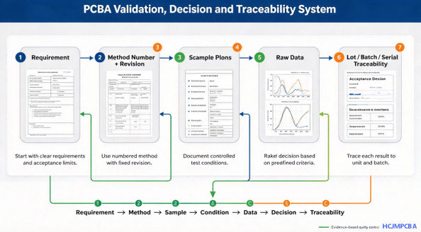
Engineering Verification And Quality Traceability Link Of Hcjmpcba
Different circuit board constructions serve different engineering purposes.
| PCB Type | Typical Application | Main Consideration |
|---|---|---|
| Single-sided PCB | Simple control and low-complexity circuits | Routing space and electrical requirements |
| Double-sided PCB | General electronics and control boards | Routing density and plated-through connections |
| Multilayer PCB | Complex digital systems and industrial controllers | Stack-up, signal integrity, and manufacturing complexity |
| Flexible PCB | Compact or moving electronic assemblies | Bend requirements and mechanical reliability |
| Rigid-flex PCB | Integrated rigid and flexible structures | Mechanical design and specialized fabrication requirements |
| HDI PCB | High-density electronic products | Microvias, fine features, and process capability |
| Breakout board | Device interfacing, prototyping, and signal access | Pin mapping, layout, and intended electrical function |
The correct choice depends on circuit complexity, available space, mechanical constraints, operating environment, and production cost.
Material selection should follow the electrical, thermal, mechanical, and environmental requirements of the product.
Engineers should consider operating frequency, dielectric properties, temperature exposure, board thickness, copper weight, material availability, and expected service conditions.
For high-speed designs, the dielectric structure and copper geometry may affect impedance and signal integrity. For power electronics, conductor geometry and thermal behavior may be more important. Flexible circuits introduce additional mechanical considerations.
The material and stack-up should therefore be approved before manufacturing rather than left to an undocumented assumption
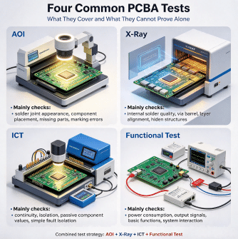
Comparison Of Aoi X Ray Ict And Functional Testing In Pcba Manufacturing
PCB fabrication converts approved design data into a physical bare board. The exact manufacturing sequence varies with board construction, but the following stages explain the main principles.
The manufacturer selects the specified base material and copper-clad laminate according to the approved stack-up, thickness, copper requirements, and applicable material specifications.
Material identification and production documentation help prevent incorrect material or construction from entering the manufacturing process.
The intended circuit pattern is transferred to the copper surface through an appropriate imaging process.
Unwanted copper is then removed through etching, leaving the conductive traces and other copper features defined by the design.
Process variation can affect trace width, spacing, and conductor integrity. For this reason, the manufactured circuit pattern must be checked against the applicable design requirements.
Drilling creates the required holes. Where electrical connections between layers are required, plated-through-hole processes provide conductive connections through the board structure.
Hole diameter, position, plating requirements, and layer connectivity depend on the approved design and performance specification.
The solder mask protects designated areas of the PCB and defines openings for solderable pads.
The surface finish is selected according to requirements such as solderability, component assembly, storage conditions, and the intended application.
These requirements should be specified in the manufacturing documentation rather than assumed to be identical for every PCB.
The board outline is formed using the specified profiling method. Final inspection may include dimensions, visual checks, and applicable electrical tests.
Inspection criteria should be based on the approved drawing, applicable performance specification, and customer requirements.
A bare-board acceptance decision should be supported by the inspection and test methods appropriate to the product.
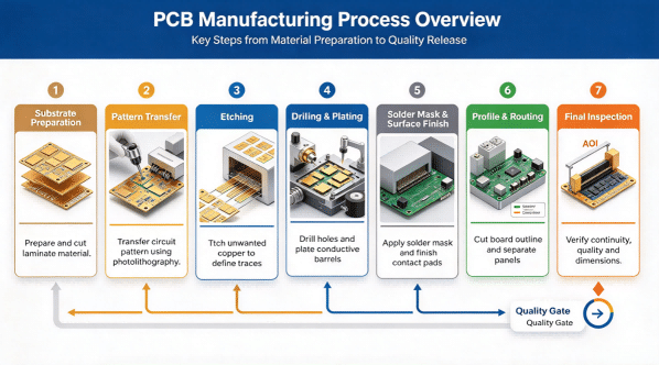
Printed Circuit Board Fabrication Process From Material Preparation To Final Inspection
Bare-board fabrication is only one part of producing a functional electronic assembly. The assembly process must also control component identity, placement, soldering, inspection, and testing.
Before assembly, the production team should review the BOM against the approved component specifications and assembly data.
Key checks include manufacturer part numbers, package types, approved substitutions, component orientation, polarity, and handling requirements.
If a component is unavailable, the proposed alternative should be reviewed and approved according to the agreed change-control process. A similar package does not automatically mean that an alternative component is electrically or mechanically equivalent.
Solder paste printing deposits solder paste onto designated PCB pads before SMT placement.
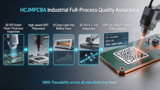
Three-dimensional solder paste inspection (3D SPI), where included in the production process, can assess characteristics such as paste volume, height, and position against configured inspection criteria.
This information can help identify printing variation before it contributes to downstream soldering defects.
Pick-and-place equipment positions components according to the approved placement program and component orientation data.
The program must correspond with the PCB footprint, BOM, component package, polarity, and intended circuit connections.
During reflow soldering, the temperature profile must be suitable for the solder paste, components, PCB construction, and applicable process requirements.
A single unverified profile should not be assumed to suit every assembly.
Depending on the design, through-hole components may be assembled using wave soldering, selective soldering, or other suitable methods.
After soldering, inspection requirements should reflect component technology and product risk.
HCJMPCBA’s PCBA workflow can incorporate SMT and through-hole assembly, 3D SPI, AOI, ICT, and X-ray inspection according to the project scope and applicable process requirements.
The purpose is to establish a suitable production and inspection plan for the specific assembly rather than to apply every inspection method automatically to every product.
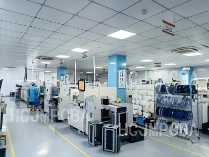
Hcjmpcba Smt
No single inspection method can identify every possible PCB or PCBA defect. The correct combination depends on the design, product risk, test coverage, production volume, and acceptance requirements.
| Method | Primary Purpose | Typical Application | Important Limitation |
|---|---|---|---|
| AOI | Optical inspection of visible features | Component presence, position, orientation, and visible solder-related defects | Cannot verify every electrical fault or hidden joint |
| X-ray / AXI | Inspection of internal or hidden structures | BGA and other joints that are difficult to inspect optically | Does not replace electrical or functional testing |
| ICT | Electrical checks at defined circuit test points | Component and circuit verification where access and coverage are appropriate | Coverage depends on fixture, access, and test design |
| Flying Probe | Electrical testing using moving probes | Prototypes and lower-volume boards where suitable | Test time and coverage depend on the design and program |
| Functional Test | Verification of specified product behavior | Confirming defined operating functions | Only verifies the functions and conditions included in the test |
AOI is useful for identifying visible placement and soldering issues. X-ray inspection can reveal certain hidden structures. ICT and flying-probe testing evaluate electrical characteristics within their respective test coverage, while functional testing checks whether the assembly behaves as specified under defined operating conditions.
These methods are complementary rather than interchangeable.
For example, a board may pass visual inspection but still contain an electrical open circuit. Conversely, an electrical test may pass while a cosmetic or workmanship issue remains that must be assessed against the applicable acceptance criteria.
Printed Circuit Board Fabrication Process From Material Preparation To Final Inspection
A quality requirement becomes useful when it can be translated into a defined method, measurable conditions, and an objective acceptance decision.
For OEM engineers and procurement teams, this is often the difference between a general quality promise and a verifiable production agreement.
| Verification Item | Method or Reference | Conditions to Define | Evidence to Retain |
|---|---|---|---|
| PCB dimensions | Approved drawing and measurement method | Datum, tolerance, and measurement procedure | Measurement records |
| Bare-board electrical integrity | Approved electrical test procedure | Test coverage, limits, and acceptance criteria | Electrical test results |
| Controlled impedance | Applicable impedance test method, where required | Target impedance, tolerance, and test structure | Impedance report |
| Solder paste deposition | SPI inspection plan, where applicable | Inspection settings and limits | SPI results |
| Solder joint workmanship | Agreed workmanship criteria | Applicable standard, class, and revision | Inspection records |
| Circuit behavior | ICT or functional test procedure | Inputs, loads, operating conditions, and limits | Measured results and pass/fail records |
| Production traceability | Defined identification and record process | Lot, batch, serial number, or work order | Traceability records |
The specific methods and records should be agreed upon before production. A requirement should not be assumed to apply simply because it appears in a general manufacturing checklist.
A statement such as “inspect according to IPC standards” may not fully define the acceptance requirements.
A controlled specification should identify the applicable standard or method number, revision or issue level, relevant acceptance criteria, and any customer-specific requirements.
For example, IPC-2221 addresses general printed-board design, while IPC-6012 addresses qualification and performance requirements for rigid printed boards. IPC-A-610 addresses acceptability of electronic assemblies. These documents serve different purposes and should not be treated as interchangeable.
The applicable version should be confirmed against the project specification and current official standards information.
A sample plan should specify the inspection or test item, sample quantity or frequency, selection method, acceptance criteria, and response to a nonconforming result.
The plan may differ according to product risk, production volume, customer requirements, process history, and applicable standards.
There is no single sample quantity that is appropriate for every PCB or PCBA project.
A test result marked only “PASS” provides limited information if the test conditions and acceptance limits are unknown.
Where required, records should identify the test method, relevant equipment or program, test conditions, measured values, acceptance limits, and final result.
Traceability can then connect the relevant records to a production lot, batch, serial number, or work order.
This makes it easier to investigate recurring defects, evaluate affected production, and support corrective-action decisions.
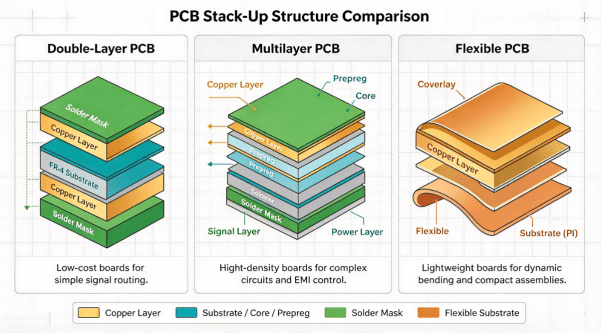
Comparison Of Pcb Types And Multilayer Printed Circuit Board Stack Up Structures
The following example can be adapted for an RFQ, purchase order, or quality agreement. It should be reviewed against the actual project requirements before use.
- The supplier shall manufacture the PCB/PCBA according to the customer-approved fabrication data, BOM, assembly drawings, specifications, and revision-controlled documents.
- Applicable inspection and test methods, including method numbers, revisions, sampling plans, test conditions, and acceptance criteria, shall be agreed upon before production.
- Required test records shall identify the inspection or test performed and retain the agreed measured results, raw data, and pass/fail decisions.
- Production records shall maintain agreed traceability to the applicable lot, batch, serial number, or work order.
- Any proposed material, process, or document change affecting product conformity shall be reviewed and approved according to the agreed change-control procedure.
This clause helps establish clear expectations before production begins. It does not replace a detailed technical specification or a project-specific quality agreement.
Missing stack-up details, drill data, or assembly information can force assumptions during quotation or manufacturing.
Prevention: Use a document checklist before releasing the project for production.
An outdated Gerber file or BOM can result in a product that does not match the customer’s latest approved design.
Prevention: Identify approved document revisions and maintain controlled change records.
AOI cannot independently verify every electrical fault, hidden solder joint, or product function.
Prevention: Select inspection and testing methods according to the actual defect risks and required coverage.
A generic test statement does not explain what was measured, under which conditions, or against which acceptance criteria.
Prevention: Define the method, test conditions, acceptance limits, and required records before production.
If a recurring defect occurs, missing lot or production information can make it difficult to identify the affected units.
Prevention: Agree on traceability fields and record-retention requirements at project launch.
A successful prototype does not automatically prove that the production documents, material supply, manufacturing tolerances, and inspection plan are ready for volume production.
Before scaling, confirm the approved design revision, component availability, sample verification requirements, and production test plan.
For projects with multiple board variants and frequent engineering changes, clear BOM control and revision identification are especially important.
Each production order should reference the applicable design, assembly, and testing requirements.
Medical electronics, automotive electronics, industrial controls, and other quality-sensitive products may require additional controls according to their intended use and applicable customer or industry requirements.
A supplier’s equipment or certification should not be treated as automatic proof that every individual product meets every application-specific requirement.
When the same defect appears repeatedly, investigation should consider design, materials, process parameters, equipment setup, inspection methods, and changes to production data.
Traceable records provide the evidence needed to support root-cause analysis and corrective action.
Before committing to production, procurement teams and engineering teams can ask which of the following records are available for their specific project:
Not every record is necessary for every product, and not every record is automatically included in a standard quotation.
A capable manufacturing partner should be able to explain which evidence is available, what it demonstrates, and which additional requirements need to be agreed upon before production.
The objective is not to request the largest possible volume of documentation. It is to obtain the evidence necessary to verify product conformity and manage the risks relevant to the project.
Guangzhou Huachuang Precision Technology Co., Ltd. operates under the brand HCJMPCBA and supports PCB assembly projects involving engineering review, component assembly, inspection, and testing according to project requirements.
For suitable projects, the manufacturing workflow can incorporate turnkey or consigned PCBA, SMT and through-hole assembly, 3D SPI, AOI, ICT, and X-ray inspection.
The appropriate process configuration depends on the board design, component technology, production quantity, inspection requirements, and agreed scope of work.
Before production, the engineering and manufacturing teams need sufficient information to evaluate the project. This may include Gerber files, drill data, PCB stack-up, BOM, assembly drawings, quantity, target schedule, and required testing specifications.
For more complex or quality-sensitive assemblies, customers should define the required inspection methods, applicable method numbers and revisions, sample plans, test conditions, acceptance criteria, raw-data requirements, and traceability fields before production begins.
This approach connects the design intent with the actual manufacturing and verification process. It also gives both the customer and the manufacturer a clearer basis for resolving technical questions, managing changes, and evaluating production results.
The central principle is simple: manufacturing requirements should be defined before production, inspection should match the risks, and quality claims should be supported by appropriate evidence.
The PCB manufacturing process typically includes material preparation, circuit pattern formation, drilling, plating, solder mask application, surface finishing, profiling, and final inspection. The exact sequence depends on board construction, technology, and the approved manufacturing specifications.
PCB printing may refer to a specific printing or circuit-pattern transfer operation. PCB fabrication is the broader process of manufacturing a bare printed circuit board. PCBA assembly is a separate stage in which electronic components are mounted and soldered onto the PCB.
A PCB is the printed circuit board that provides the conductive interconnections and mechanical support for electronic components. A PCBA is a populated board with electronic components assembled and soldered onto it. Depending on the product, a completed PCBA may require additional electrical or functional testing.
Common requirements include approved fabrication data, NC drill files, PCB stack-up, material specifications, board dimensions, copper requirements, and relevant tolerances. PCBA projects generally also require a BOM, assembly drawings, component information, and applicable testing requirements.
The applicable standards depend on the board technology and product requirements. IPC-2221 addresses general printed-board design, while IPC-6012 addresses qualification and performance requirements for rigid printed boards. Assembly workmanship and other requirements may involve additional standards. The appropriate document and revision should be confirmed for each project.
AOI checks visible features, X-ray can inspect certain hidden structures, ICT and flying-probe methods evaluate electrical characteristics within their coverage, and functional testing verifies specified product behavior. The appropriate combination depends on the design, test coverage, product risk, and customer requirements.
Useful records may include approved document revisions, sample inspection results, defined test methods and conditions, acceptance criteria, measured data, and agreed production traceability. The required record set should be established before production rather than assumed to be identical for every project.
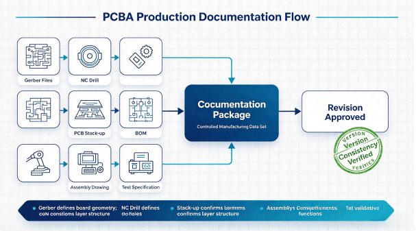
Pcb Design Package Review And Revision Control Before Manufacturing
Understanding printed circuit board processes means understanding more than how copper patterns are formed or components are soldered.
A reliable manufacturing plan connects the approved design with material selection, fabrication, assembly, inspection, testing, and production records.
For engineering teams, the priority is to define manufacturability and verification requirements before production. For procurement teams, the priority is to confirm that the supplier can explain the process, identify applicable acceptance criteria, and provide the agreed evidence.
For more information about PCBA services, please contact Guangzhou Huachuang Precision Technology(HCJMPCBA).
Update triggers: standard revision changes / recurring questions / production checklist updates.
Explore the definitive guide to pcb assembly—from turnkey pcb assembly to smt pcb assembly and thr
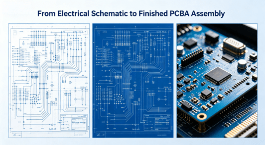
Learn what an electrical schematic is, how to read a circuit diagram, and how PCB/PCBA manufacturing
Discover how to master simple electronic circuit projects for beginners and transition seamlessly to