7-Fundamental Stages of the PCB Manufacturing Process: A Precision Guide by HCJMPCBA
Explore the PCB Manufacturing Process from design and imaging to etching, drilling, plating, and fin

An electrical schematic is a symbolic representation of an electronic circuit showing electrical relationships, signal paths, and component functions instead of physical placement. Engineers use schematic diagrams, wiring diagrams, and PCB schematics to design, verify, manufacture, troubleshoot, and validate electronic products before PCB fabrication and PCBA assembly begin. Industry-standard schematic practices are defined by organizations such as IPC and IEC.
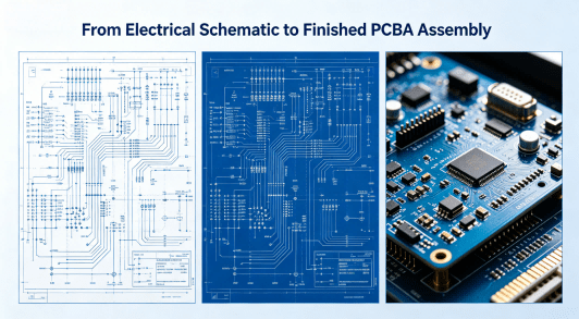
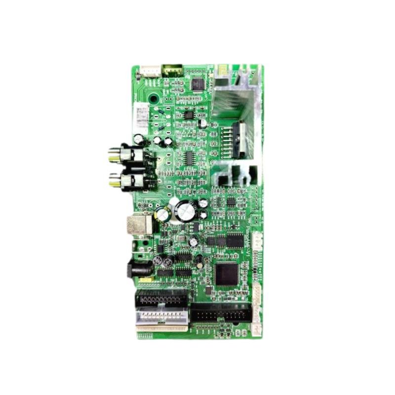
From Hcjmpcba Electrical Schematic To Finished Pcba Assembly
An electrical schematic (also called a schematic diagram, circuit schematic, or electrical diagram) is a simplified graphical representation of an electronic system using standardized symbols instead of realistic component drawings.
Unlike an electrical wiring diagram, a schematic drawing does not focus on physical wire positions or exact PCB routing. Its primary purpose is to communicate electrical logic, signal relationships, power distribution, and circuit functionality.
In electronics manufacturing, the schematic diagram becomes the foundation for:
Modern PCB and PCBA manufacturing workflows rely heavily on schematic accuracy because even a small net labeling error or missing pull-up resistor can create intermittent failures during mass production.
According to IEC schematic standards and IPC documentation practices, schematic readability and revision control are critical for manufacturing consistency.
| Document Type | Primary Purpose | Used By | Shows Physical Placement | Manufacturing Relevance |
|---|---|---|---|---|
| Schematic Diagram | Electrical logic and signal relationships | Electrical engineers | No | Very High |
| Wiring Diagram | Physical cable/wire connections | Installers and technicians | Partially | Medium |
| PCB Layout | Physical routing and placement | PCB designers and manufacturers | Yes | Critical |
| Assembly Drawing | Component placement reference | SMT operators and QA | Yes | High |
A common mistake among new engineers is confusing a wiring schematic diagram with a PCB layout. A schematic circuit diagram explains “how the circuit works,” while PCB files define “how the board is physically manufactured.”
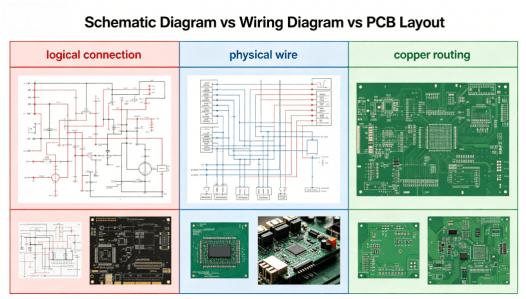
Hcjmpcba Schematic Diagram Vs Wiring Diagram Vs Pcb Layout
Understanding how to read electrical schematics is one of the most important engineering skills in PCB development and electronics manufacturing.
Most circuit diagrams start with power distribution.
Common labels include:
Power integrity problems during PCB assembly often originate from incorrect grounding strategies or mixed analog/digital ground handling.
Most schematic diagrams follow left-to-right signal flow:
For example:
This structure simplifies troubleshooting and helps engineers understand functional relationships quickly.
Standard reference prefixes include:
| Prefix | Component |
|---|---|
| R | Resistor |
| C | Capacitor |
| L | Inductor |
| D | Diode |
| Q | Transistor |
| U | IC / MCU |
| J | Connector |
Reference designators are essential for:
A simple circuit diagram may include:
Standardized symbols improve communication across PCB design teams, contract manufacturers, and OEM buyers.
Many beginners incorrectly assume lines represent physical wires.
In reality:
This is especially important in multilayer PCB schematic designs.
One of the most common PCBA production problems occurs when:
do not match.
At HCJMPCBA, engineering review includes cross-verification between:
before SMT production approval.
Professional OEM manufacturing should always maintain:
Using outdated schematic drawings during mass production can result in:
Controlled revision management is particularly important for industrial control boards, medical electronics, and AI hardware systems.
Well-designed PCB schematics include:
These improve:
Some circuits may function electrically but still be difficult to manufacture reliably.
Examples include:
This is why experienced PCBA manufacturers perform DFM analysis before production release.
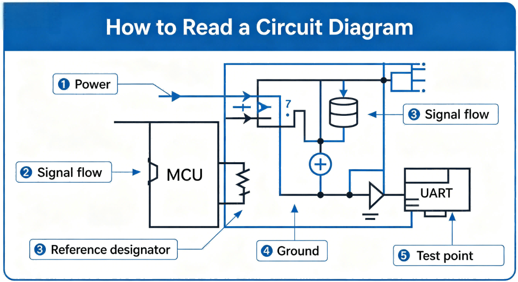
How To Read A Circuit Diagram Hcjmpcba
A PCB manufacturing workflow typically begins with the electrical schematic and progresses through multiple engineering and production stages.
Engineers create the circuit schematic using EDA software such as:
This stage defines electrical behavior and connectivity.
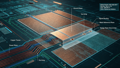
PCB designers convert the electrical schematic into a physical board layout including:
Manufacturing engineers verify:
This reduces manufacturing defects before PCB fabrication begins.
Outputs usually include:
These files become the manufacturing package for PCB and PCBA suppliers.
PCB fabrication processes include:
Surface finishes may include:
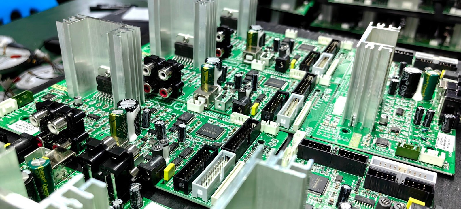
SMT production generally includes:
At HCJMPCBA, process records can be linked to:
for controlled manufacturing projects.
Typical verification methods include:
Production reliability depends heavily on verification quality rather than only SMT placement speed.
For higher reliability projects, manufacturers may maintain:
These records are especially valuable during:
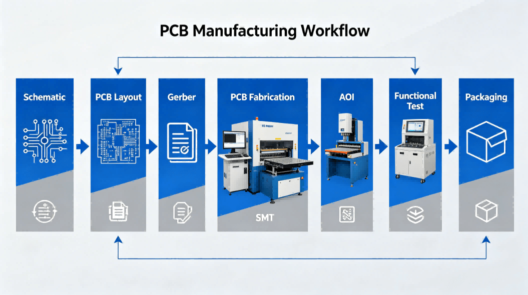
Hcjmpcba Pcb Manufacturing Workflow
| Requirement | Wiring Diagram | Electrical Schematic | PCB Layout |
|---|---|---|---|
| Troubleshooting electrical logic | Limited | Excellent | Moderate |
| PCB manufacturing | Limited | Required | Critical |
| Cable installation | Excellent | Limited | No |
| SMT assembly | No | Moderate | Critical |
| Failure analysis | Moderate | Excellent | High |
| Functional verification | Moderate | Excellent | Moderate |
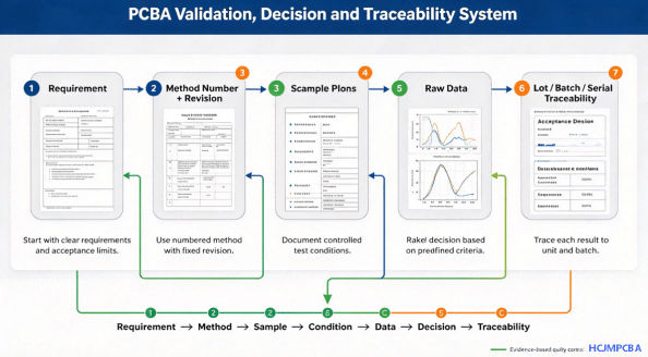
| Verification Item | Evidence | Why It Matters |
|---|---|---|
| Revision Control | Method number + revision record | Prevents outdated builds |
| Sample Plan | Inspection sampling criteria | Reduces batch risk |
| Test Conditions | Voltage/current/environment records | Improves reproducibility |
| AOI/X-Ray Reports | Inspection images | Detects solder defects |
| Raw Data | Measurement and process logs | Supports root cause analysis |
| Traceability | Lot/batch/serial records | Enables failure tracking |
| Functional Test | Pass/fail criteria and data | Verifies real-world operation |
At HCJMPCBA, engineering and production records may be associated with revision-managed manufacturing documentation to reduce uncontrolled production changes during PCB and PCBA assembly.

Hcjmpcba Traceability & Verification Flow
Mistake 1 — Confusing Physical Routing with Electrical Logic
A schematic drawing explains electrical relationships, not PCB copper routing.
Mistake 2 — Ignoring Ground Separation
Mixed analog and digital grounds can create EMI and signal integrity problems.
Mistake 3 — Missing Net Labels
Incorrect or duplicated net names can create hidden electrical failures.
Mistake 4 — Using Outdated Revisions
Old schematic revisions remain one of the most common causes of manufacturing errors.
Mistake 5 — Sending Incomplete Manufacturing Packages
Some OEM buyers provide only:
This significantly increases PCBA production risk.
In one industrial control project, prototype boards passed functional testing successfully, but intermittent communication failures appeared during volume production.
Root cause analysis later identified:
The issue was resolved by:
This type of problem is common when engineering data management is weak.
OEM buyers can reduce manufacturing risk by requesting:
Reliable suppliers should be able to explain how manufacturing records connect to:
These engineering and verification methods are commonly used in:
Higher reliability products generally require stronger revision management and traceability systems.
What is a schematic diagram?
A schematic diagram is a symbolic representation of an electrical or electronic circuit showing functional electrical relationships.
How do you read a circuit diagram?
Start by identifying power rails, ground, signal flow, component references, and net labels before analyzing functional blocks.
What is the difference between a wiring diagram and a schematic?
A wiring diagram shows physical wiring connections, while a schematic focuses on electrical logic and circuit functionality.
What is a PCB schematic?
A PCB schematic is the logical electrical design used to create PCB layouts and manufacturing files.
How are printed circuit boards manufactured?
PCB manufacturing includes imaging, etching, drilling, plating, solder mask application, surface finishing, and electrical verification.
Why is revision control important in PCBA manufacturing?
Revision control prevents outdated manufacturing files from being used during production and reduces engineering change risks.
What traceability records should a PCB assembly supplier provide?
Common records include:
Understanding how to read electrical schematics is fundamental to successful PCB design and PCBA manufacturing.
A schematic diagram defines electrical intent, while PCB fabrication and assembly convert that intent into a manufacturable product. In modern electronics production, manufacturing success depends not only on circuit functionality but also on:
For OEM buyers and engineers, requesting production evidence and manufacturing verification records is often more valuable than comparing quotations alone.
For more information about PCBA services, please contact Guangzhou Huachuang Precision Technology (HCJMPCBA).
Update triggers: standard revision changes / recurring questions / production checklist updates.
Explore the PCB Manufacturing Process from design and imaging to etching, drilling, plating, and fin
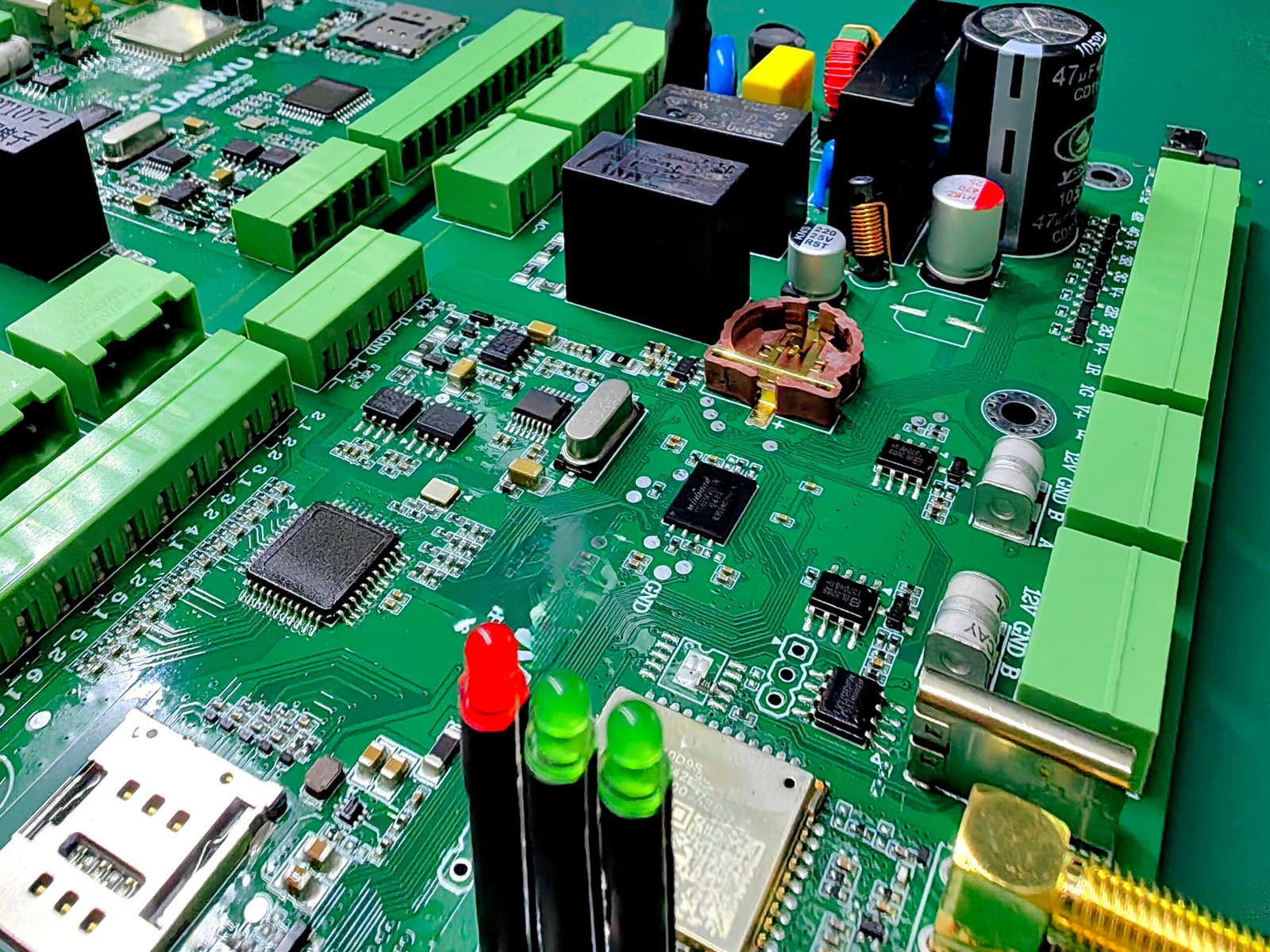
Discover a custom pcb design framework in 10 strategic steps—covering cost estimation, layout best
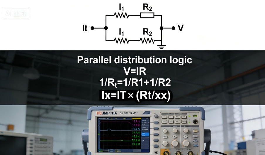
This guide breaks down the current divider and voltage divider formulas, explaining their core diffe