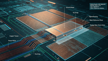
Revolutionizing Machine Learning Systems with Advanced Rigid-Flex PCB Technology
Guangzhou Huachuang Precision Technology Co., Ltd. (Huachuang Precision) specializes in advanced rig

For hardware engineers and procurement professionals, managing a PCB project typically means juggling multiple vendors: one for bare board fabrication, another for component sourcing, a third for assembly, and perhaps a fourth for testing. Each additional vendor introduces coordination overhead, shipping delays, quality variation, and communication gaps.
A full-service PCB manufacturing provider consolidates these steps into a single, integrated workflow. From bare board fabrication through SMT assembly, testing, and final delivery, the entire process is managed under one roof — with one point of contact, one quality standard, and one timeline.
At Guangzhou Huachuang Precision Technology Co., Ltd. (HCJMPCBA), we offer exactly this integrated model. With nearly 3,500 m² of ESD‑protected manufacturing space, multiple high-speed SMT lines, and ISO9001 quality management and ISO13485 medical device quality management certifications, we provide end-to-end PCB manufacturing and assembly services for industrial control, medical devices, automation, and power electronics applications.
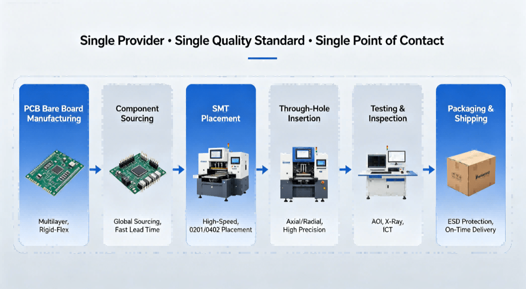
Panoramic View Of Integrated Pcb Manufacturing Services
A full-service PCB manufacturer must support a broad range of board types to serve diverse applications. Our fabrication capabilities cover:
Rigid PCBs — The most common board type, available in standard FR4 and high-Tg materials. Suitable for most industrial, consumer, and medical applications.
Flex PCBs and Rigid-Flex PCBs — Flexible circuits that bend and fold to fit tight spaces or moving assemblies. Rigid-flex combines rigid sections for component mounting with flexible sections for interconnection, reducing connectors and improving reliability.
Heavy Copper PCBs — Boards with 3–6 oz copper pours for high-current power conversion, motor drives, and industrial power supplies. Heavy copper requires specialized etching and soldering processes.
Aluminum-Backed and Metal Core PCBs (MCPCB) — Designed for high-power LED and power electronics applications where thermal dissipation is critical. The metal core acts as a heat spreader.
High-Frequency PCBs — Using low-loss materials such as RO4003C, RO4350B, RO3003, and RT5880 for RF and microwave applications. These materials maintain consistent dielectric properties at high frequencies.
HDI PCBs — High-density interconnect boards with fine lines, microvias, and buried/blind vias for compact, high-component-density designs.
Custom-Shaped PCBs — Beyond standard rectangles, we fabricate circular, irregular, and panelized shapes to meet specific mechanical enclosure requirements.
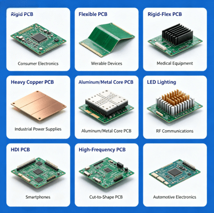
Pcb Type Matrix Diagram
Material selection directly impacts electrical performance, thermal management, and manufacturability. Our material capabilities include:
Standard FR4 — Tg 140°C, the industry workhorse for general-purpose applications.
High-Tg FR4 — Tg 170°C and Tg 180°C for applications requiring higher thermal stability, such as automotive and industrial electronics.
High-Frequency Laminates — RO4003C, RO4350B, RO3003, RO3010, and RT5880 from Rogers, plus other low-loss materials for RF and high-speed digital designs. These materials maintain stable dielectric constants across frequency and temperature.
Metal Core — Aluminum core (domestic 1060) and copper core for enhanced thermal dissipation.
Flexible Substrates — DuPont PI (polyimide) materials including PI25UM, plus domestic Shengyi PI for flex and rigid-flex applications.
All materials are available in RoHS-compliant versions, and we support both lead-free and tin-lead assembly processes.
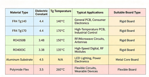
Comparison Of Common Pcb Materials
Our manufacturing infrastructure is designed for both flexibility and scale. Key capabilities include:
Layer Count — 1 to 32 layers, supporting everything from simple single-sided boards to complex multilayer designs.
Maximum Panel Size — 400mm × 450mm, accommodating most standard board dimensions.
Lead Time — Prototype lead times starting from as fast as 2 days; production lead times vary by volume and complexity.
Quick Turn Service — Expedited prototyping for time-critical NPI programs.
Prototype and Production Quantities — From pilot runs of a few boards to mass production of tens of thousands per month, with consistent quality standards across all volumes.
Advanced Via Structures — Blind vias, buried vias, and microvias (both stacked and staggered configurations) for HDI designs.
Via-in-Pad — Vias placed directly in component pads, typically filled with conductive or non-conductive epoxy and copper-capped for planar surfaces.
Via Treatment Options — Via tenting (covered with solder mask), via plugging/filling with resin, and via filling with conductive material.
Special Features — Gold fingers for edge connectors, press-fit holes, countersink/counterbore holes, half-cut/castellated holes for module edge connections, peelable solder mask for selective soldering areas, edge plating, carbon mask for keypad contacts, and Kapton tape for specific masking requirements.
Impedance Control — Controlled impedance routing with tolerance of ±10%. We adjust layer stackup, dielectric thickness, and trace geometry to meet your impedance specifications.
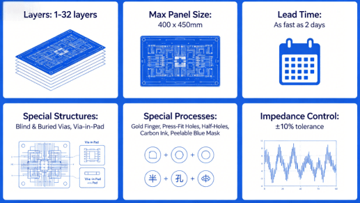
Overview Of Pcb Manufacturing Capabilities
The choice of surface finish affects solderability, shelf life, cost, and compatibility with assembly processes. We offer the following finishes:
HASL (Hot Air Solder Leveling) — The traditional finish, providing excellent solderability at low cost. Available in both tin-lead and lead-free (RoHS) versions.
ENIG (Electroless Nickel Immersion Gold) — A two-layer finish with nickel barrier and thin gold layer. Provides excellent flatness, good solderability, and long shelf life. RoHS-compliant. Ideal for fine-pitch components and aluminum wire bonding.
ENEPIG (Electroless Nickel Electroless Palladium Immersion Gold) — Adds a palladium layer between nickel and gold, providing additional corrosion resistance and compatibility with both soldering and wire bonding (aluminum and gold). RoHS-compliant.
Immersion Silver — A thin silver layer over copper. RoHS-compliant, excellent flatness, good solderability, and lower cost than ENIG. Suitable for high-frequency applications.
Immersion Tin — A thin tin layer over copper. RoHS-compliant, good solderability, and flat surface. Suitable for press-fit applications.
OSP (Organic Solderability Preservatives) — An organic coating that protects copper from oxidation. RoHS-compliant, low cost, and excellent flatness. Requires careful handling and has limited shelf life.
Each finish has trade-offs in cost, shelf life, flatness, and process compatibility. Our engineering team can help you select the optimal finish for your application and assembly process.
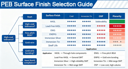
Surface Treatment Selection Guide
Our manufacturing capabilities are defined by precise specifications and tolerances:
| Layer Count | Typical Value (mm) | Ultimate Value (mm) |
|---|---|---|
| 1-layer & 2-layer | 0.40 | 0.20 |
| 4-layer | 0.40 | 0.30 |
| 6-layer | 0.60 | 0.40 |
| 8-layer | 1.00 | 0.80 |
| 10-layer | 1.20 | 1.00 |
| 12-layer | 1.80 | 1.20 |
| 14-layer | 2.20 | 1.60 |
| 16-layer | 2.50 | 1.80 |
| Copper Weight | Wire-to-Wire / Wire-to-Copper | Wire-to-Via | Wire-to-Pad | Wire-to-Text |
|---|---|---|---|---|
| 1 oz | 4.0 mil (typ) / 3.5 mil (ult) | 8.0 / 6.0 | 10.0 / 8.0 | 5.0 / 4.0 |
| 2 oz | 8.0 / 7.0 | 10.0 / 9.0 | 10.0 / 9.0 | 6.0 / 5.0 |
| 3 oz | 10.0 / 9.0 | 14.0 / 13.0 | 14.0 / 13.0 | 7.0 / 6.0 |
| 4 oz | 13.0 / 12.0 | 16.0 / 15.0 | 16.0 / 15.0 | 8.0 / 7.0 |
| 5 oz | 16.0 / 15.0 | 20.0 / 19.0 | 20.0 / 19.0 | 8.0 / 7.0 |
| 6 oz | 18.0 / 17.0 | 24.0 / 23.0 | 24.0 / 23.0 | 10.0 / 9.0 |
Colors: Green, White, Blue, Black, Red, Yellow
Thickness: 10μm – 12μm
Placement Tolerance: ±1.5 mil
Character Height: 30 mil (typical)
Character Width: 5 mil (typical)
For aluminum PCBs, MCPCBs, flex PCBs, rigid-flex PCBs, and other advanced boards, clearance specifications may vary. Our engineering team provides case-by-case guidance.
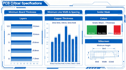
Key Specification Parameter Information Of Pcb
The distinction between “PCB manufacturing” and “PCBA” is often blurred in practice. A full-service provider handles both:
Bare Board Fabrication — All the capabilities described above: material selection, layer stacking, drilling, plating, etching, solder mask, surface finish, and routing.
Component Sourcing — Full BOM procurement from authorized distributors, with proactive management of long-lead and obsolete parts.
SMT Assembly — High-speed pick-and-place, reflow soldering with closed-loop temperature control, and nitrogen atmosphere capability for demanding assemblies.
Through-Hole Assembly — Selective wave soldering for mixed-technology boards with through-hole connectors, inductors, and transformers.
Testing — AOI, X-ray inspection (for BGAs, QFNs, and power modules), ICT, and functional testing — all in-house.
Packaging and Shipping — ESD-safe packaging and logistics coordination.
By consolidating fabrication and assembly under one roof, we eliminate the coordination overhead of managing separate vendors and reduce the risk of quality issues that arise when bare boards are shipped between facilities.
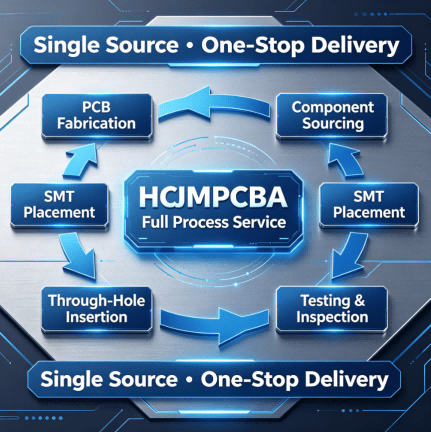
Integrated Pcb Fabrication And Assembly Process
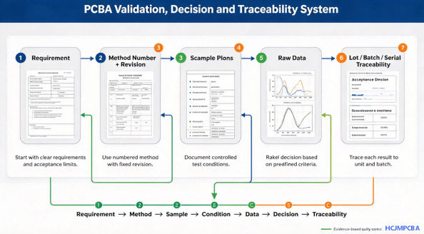
Our quality system is built on documented processes, continuous monitoring, and full traceability:
ISO9001 Certification — Quality management system covering all manufacturing and assembly processes.
ISO13485 Certification — Medical device quality management, ensuring compliance with the rigorous requirements of the medical industry.
Material Traceability — Every component and material lot is logged with manufacturer, date code, and batch information. Our intelligent MES system provides UID-level traceability.
In-Process Inspection — 3D SPI for solder paste verification, AOI after reflow, X-ray for hidden joints, and ICT/functional testing for electrical validation.
Statistical Process Control — Key process parameters are monitored in real time to detect and correct drift before defects occur.
Documentation — Complete quality records, test reports, and certificates of compliance provided with every order.
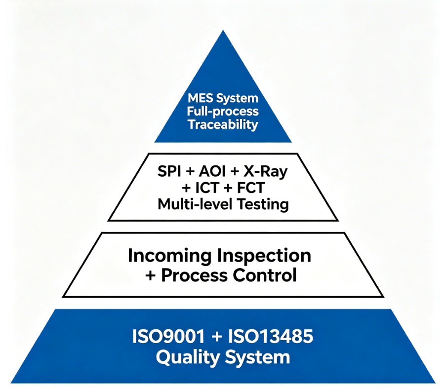
Schematic Diagram Of Quality Management System
One of the most critical transitions in product development is moving from prototype quantities — where boards may be hand-inspected with extra attention — to volume production, where consistency and repeatability are paramount.
Our manufacturing infrastructure supports both ends of this spectrum:
Prototype Runs — Fast turnaround, flexible process setup, and no minimum order quantity. Ideal for NPI and design validation.
Pilot Runs — 50 to 500 units, with full process documentation and first-article inspection.
Volume Production — Tens of thousands of boards per month, with consistent quality, SPC monitoring, and on-time delivery.
The same engineering team, production line, and quality system serve all volumes — so the process that validates your prototype is the same process that delivers your production boards.
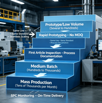
Seamless Scaling From Prototype To Mass Production
Starting a PCB project with a full-service manufacturer is straightforward:
Submit your design files — Gerber, drill files, and BOM.
Specify your requirements — Layer count, material, surface finish, copper weight, impedance control, and any special features.
Receive a quote — We provide transparent pricing with engineering costs separated from unit costs.
First-article qualification — The first board is fully inspected before production continues.
Production and delivery — Boards are manufactured, assembled, tested, and shipped to your schedule.
Our engineering team is available to review your files, identify potential manufacturing issues, and provide recommendations before production begins.
Guangzhou Huachuang Precision Technology Co., Ltd. (HCJMPCBA) — Your full-service PCB manufacturing and assembly partner from prototype to production.
Guangzhou Huachuang Precision Technology Co., Ltd. (Huachuang Precision) specializes in advanced rig
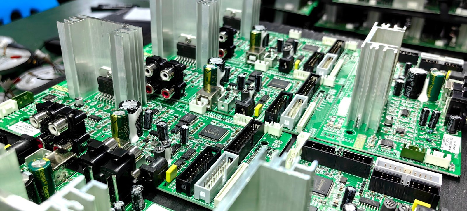
Guangzhou Huachuang Precision Technology Co., Ltd. excels in PCBA processing. It starts with order a
In the field of electronics manufacturing, PCB Layout (Printed Circuit Board Layout) is a core aspec