
Revolutionizing Machine Learning Systems with Advanced Rigid-Flex PCB Technology
Guangzhou Huachuang Precision Technology Co., Ltd. (Huachuang Precision) specializes in advanced rig
In modern electronics manufacturing, a gerber file is the fundamental blueprint that turns your digital PCB design into a physical board. Whether you design single-layer boards or complex multilayer PCBs for high-speed, high-reliability applications, gerber pcb data communicates exactly how copper traces, solder mask, silkscreen, drill holes, board outline and more should be fabricated.
Without a proper Gerber file set, even the best PCB layout cannot be manufactured accurately — mismatched layers, missing drill holes, incorrect component footprints, or misaligned solder mask are common consequences. That’s why every reputable PCB / PCBA manufacturer (like HCJMPCBA) requires a complete Gerber pack to begin production. This guide will explain what is a gerber file, what it should contain, how to generate and validate it, and what to pay attention to when you send Gerber files to a prototype or production partner.
A Gerber file is a 2D vector file format used universally in the PCB industry to describe each physical layer of a PCB — copper layers, solder mask, silkscreen, drill data, board outline, and other manufacturing information.
Each board layer is exported into a separate Gerber file, so that when processed together, all layers combine to form a complete specification of the PCB.Gerber files convert the design intent from CAD/EDA (schematics & layout) into a fabrication-ready format that PCB manufacturers and CAM machines can understand and act on.
In short: Gerber = the universal language bridging PCB design and manufacturing.
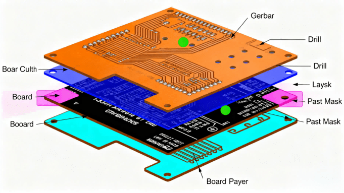
Hcjmpcba Gerber File Structure Diagram
They contain exact copper trace patterns, pad shapes, via placements, drill holes, board outline, solder mask openings, silkscreen legends — that is, everything needed to build a correct PCB.
They avoid ambiguity: unlike proprietary PCB project files (which depend on specific EDA tools), Gerber files are standard and widely supported across manufacturers globally — making them essential especially when outsourcing PCB fabrication.
For OEM engineers, procurement agents, and cross-border clients, accurate Gerber files reduce risk, lower revision cycles, and support smooth transition from prototype to mass production.
To ensure a PCB can be fabricated properly, a standard Gerber package typically includes the following layers/files. A qualified set should include all of these (unless your design omits certain layers):
Copper layers: Top copper (top signal/pads/traces), Bottom copper (bottom side), and for multilayer PCBs — internal copper layers or power/ground planes.
Solder mask layers: Top solder mask and bottom solder mask — indicating where solder-mask should protect copper, and where pads are exposed.
Silkscreen (Legend) layers: Top and bottom silkscreen (component labels, logos, reference designators, orientation marks).
Drill / Drill-hole data files: Indicating hole positions, sizes (vias, through-holes), plating requirements. Sometimes separate NC Drill (.drl) files accompany Gerber layers.
Board outline (edge cut / profile): Defines the PCB boundary — necessary for routing, panelization, mechanical fit.
Optional / Additional files depending on design — e.g. solder-paste layers (for stencil), mechanical layers, assembly drawings, if required.
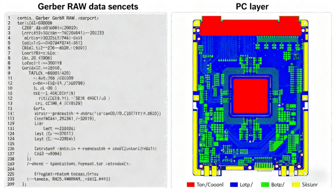
Hcjmpcba Gerber “raw Data Snippet + Pcb Layer View
The Gerber file format has evolved over decades. Today, the industry-standard format is RS-274X Extended Gerber (X-Gerber).
RS-274X (Extended Gerber / X-Gerber) — self-contained, embedding aperture definitions and layer data in one file; widely supported by modern CAM/PCB fabrication tools, and recommended for most projects.
Legacy RS-274D (Standard Gerber / old “D-code” format) — now largely obsolete; requires separate aperture files, error-prone and not recommended for modern PCB production.
HCJMPCBA strongly recommends submitting Gerber files in RS-274X format (or other fully supported standards) to ensure compatibility and minimize CAM-related errors.
To ensure your Gerber output is fabrication-ready and error-free, follow best practices. Below is a typical workflow (works in Altium, KiCad, Eagle, or most CAD/EDA tools):
Finalize your PCB layout and perform a full DRC (Design Rule Check) — ensure no overlapping copper, correct trace widths, spacing, drill sizes, and stack-up defined.
Export Gerber layers — create separate Gerber files for each required layer: copper, solder mask, silkscreen, board outline.
Export Drill / NC Drill file — including both plated through-holes, vias, and non-plated holes if any.
Name files clearly and logically (e.g. TOP.GTL, BOT.GBL, SOLDERMASK_TOP.GTS, DRILL.DRL, EDGE_CUT.GKO) — helps manufacturer avoid misinterpretation.
Zip/compress all Gerber files into one package + include README / fabrication notes — specify board thickness, copper weight, surface finish, stack-up, impedance requirements, special treatments if any.
Use a Gerber viewer (or multiple) to pre-check the files — visually inspect layers for alignment, missing pads/vias, silkscreen misplacement, board outline correctness.
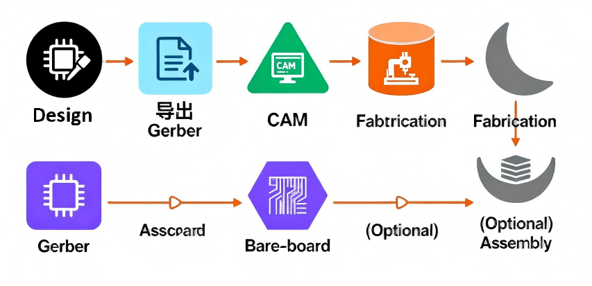
Hcjmpcba Pcb Manufacturing Process
Once your Gerber file package is received by a PCB or PCBA manufacturer, the process typically goes as follows:
Import Gerber data into CAM software, which reconstructs each layer (copper, mask, legend, drill, outline) based on vector commands.
Generate fabrication films or direct laser-imaging patterns for each copper and mask layer.
Drill/plating according to drill files, align layers, apply lamination (for multilayer boards), etch copper, apply solder mask and silkscreen, cut board outline.
After bare-board fabrication, manufacturer may proceed to PCB assembly (SMT / THT) if you provided BOM and pick-and-place data — completing PCBA.
Without accurate Gerber files, this workflow cannot operate reliably — misaligned layers or missing layer data will result in scrap boards or manufacturing delays.
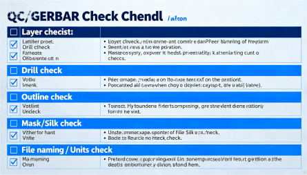
Hcjmpcba Qc Gerber Checklist Diagram
Reduce design-to-production risk: Correct Gerber export helps catch layout or layer mistakes early, avoiding failed boards or costly re-spins.
Improve communication with your PCB/PCBA vendor: A complete, well-documented Gerber package ensures clear understanding between you and the manufacturer, especially in international cooperation.
Speed up time-to-market: With clean Gerber files and efficient review, the transition from prototype to production becomes smoother and faster.
Support high-complexity boards: Multilayer, HDI, high-speed, or high-reliability PCBs all require precise layer definitions — Gerber is the universal format that supports them.
Q: What is a PCB Gerber file vs. source PCB file?
A: A source PCB file is native to your CAD software (schematic + layout + netlist + components). A Gerber file is a standardized export that contains only the physical layout data (copper, mask, silk, drill, outline) — used for fabrication.
Q: Why do I need multiple Gerber files for one PCB?
A: Because each physical layer (top copper, bottom copper, solder mask, silkscreen, drill, outline …) must be defined separately. Manufacturing equipment needs all layer data to build the final board precisely.
Q: Can I open a Gerber file to view my PCB layout?
A: Yes — there are many Gerber viewer tools (free or paid) that can load the full Gerber set and show the layout graphically. It is recommended to review before sending to manufacturer.
Q: What Gerber format should I use — RS-274X or something else?
A: Use RS-274X (Extended Gerber) — it is the current industry standard, embeds aperture and layer info, and is universally supported. Avoid outdated RS-274D if possible.
Q: What happens if my Gerber file is incomplete or incorrect?
A: PCB manufacturer may raise DFM (design-for-manufacture) issues, cause delays, scrap boards, or require revised Gerber files — resulting in cost and time waste.
Guangzhou Huachuang Precision Technology Co., Ltd. (Huachuang Precision) specializes in advanced rig

Learn 5 powerful customer communication strategies that position HCJMPCBA as one of the best PCB man

Surface Mount Technology (SMT) lies at the heart of modern electronics assembly, enabling ever‑sma


