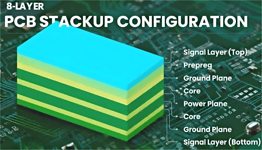
7 Key Principles: What Is an 8-Layer PCB Stackup and How to Design It Right
Discover what is an 8 layer pcb stackup, best layer configurations, materials, signal integrity stra
The NPI process (New Product Introduction) is the engineering workflow used to transition a product from prototype development to mass production. In PCB manufacturing, it includes design verification, prototype fabrication, DFM analysis, pilot production, and full-scale manufacturing.
In electronics manufacturing, moving from a PCB prototype to mass production is one of the most critical stages in product development. Many products fail during this transition because the design was not properly prepared for manufacturing.
The NPI process (New Product Introduction) ensures that a product design can be manufactured efficiently, reliably, and at scale. It bridges the gap between engineering design and large-scale production.
This guide explains how the NPI process works in real PCB and PCBA manufacturing environments and how companies can successfully scale from prototype testing to stable mass production.
The New Product Introduction (NPI) process is a structured engineering workflow that prepares a product for mass manufacturing. It validates the design, verifies manufacturability, and ensures production stability before large-scale production begins.
In PCB and PCBA manufacturing, the NPI process typically includes design verification, prototype fabrication, assembly validation, DFM optimization, and pilot production.
A well-executed NPI process significantly reduces manufacturing risks such as assembly defects, supply chain delays, and unexpected production costs.
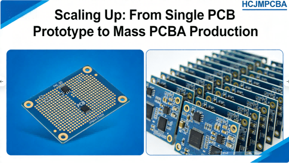
Comparison Of Pcb To Pcba Finished Products Hcjmpcba
Scaling production requires more than just increasing order quantities. It requires a gated validation process. We categorize the journey into four distinct engineering stages:
| NPI Stage | Technical Objective | Standard Reference |
|---|---|---|
| EVT (Engineering Validation) | Verifying fundamental circuit logic and signal integrity (SI). | IPC-2251 (High-Speed Design) |
| DVT (Design Validation) | Testing under environmental stress (Thermal, Vibration, EMI). | IEC 60068 Series |
| PVT (Production Validation) | Optimizing SMT line speed, First Pass Yield (FPY), and tooling. | IPC-9850 (Equipment Performance) |
| MP (Mass Production) | Continuous process control and statistical monitoring. | IPC-9191 (SPC Implementation) |
Statistical data shows that 80% of mass-production failures are rooted in design-related issues. HCJMPCBA performs a comprehensive Design for Manufacturing (DFM) audit based on IPC-7351B (Generic Requirements for Surface Mount Design and Land Pattern Standards).
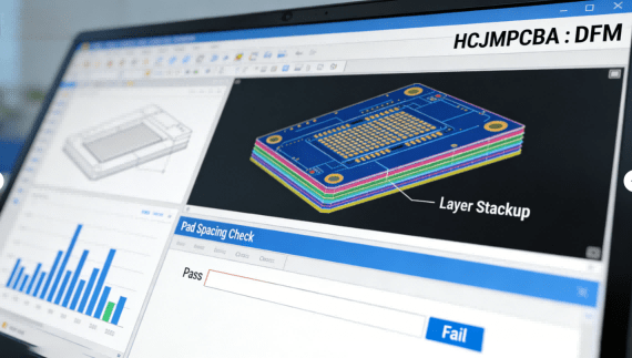
Dfm Software Analysis Interface Hcjmpcba
In mass production, component failure is often caused by improper handling rather than manufacturing defects. HCJMPCBA adheres strictly to:
To ensure zero-defect scaling, we implement automated quality gates that align with IPC-A-610G Class 3 standards for high-reliability electronics.
| Inspection Layer | Process Control Technology | Defect Prevention |
|---|---|---|
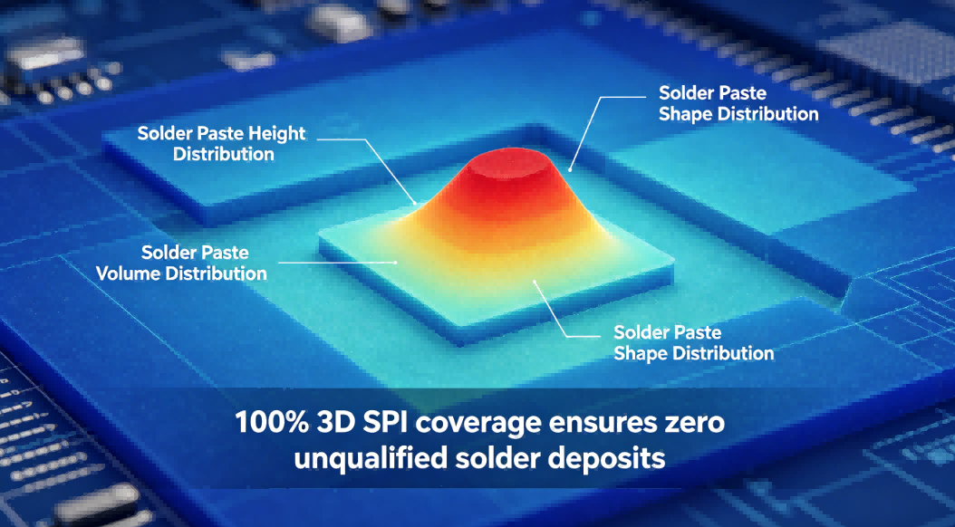
| Solder Paste (SPI) | 3D Solder Paste Inspection (Closed-Loop) | Insufficient volume, bridging, and offset. |
| Post-Reflow (AOI) | Multi-angle 3D Automated Optical Inspection | Non-wetting, lifted leads, and polarity errors. |
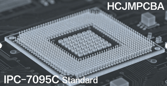
| BGA Integrity (AXI) | Automated X-Ray Inspection (2.5D/3D) | Solder voiding (limit < 25% per IPC-7095C), HiP defects. |
3d X Ray Scan Image Hcjmpcba
For mass market success, testing time must be optimized without compromising coverage. We develop custom Functional Circuit Test (FCT) jigs that simulate real-world operations, ensuring firmware and hardware synchronization. For high-density boards, we utilize In-Circuit Testing (ICT) or Flying Probe testing (per IPC-9252) to validate electrical continuity and component values.
Many electronics projects successfully produce functional prototypes but encounter serious issues when scaling production. These challenges often arise because the design was optimized for functionality rather than manufacturability.
The NPI process addresses these challenges by validating every stage of the manufacturing workflow before full production begins.
The first step of the NPI process is verifying the design files and ensuring that the PCB layout meets functional and manufacturing requirements. Engineers review Gerber files, BOM lists, and assembly drawings to confirm accuracy.
Design rule checks (DRC) and engineering reviews help identify potential problems before fabrication begins.
Once the design is verified, manufacturers produce PCB prototypes in small quantities. These prototypes allow engineers to test electrical performance, signal integrity, and thermal behavior.
Prototype testing helps detect design flaws early and reduces the risk of costly design changes later in production.
During this stage, prototype boards are assembled using SMT or through-hole assembly processes. Engineers verify component placement, solder quality, and assembly reliability.
Functional testing ensures that the assembled boards perform correctly under real operating conditions.
Design for Manufacturing (DFM) and Design for Testing (DFT) analysis are essential steps in the NPI process. Manufacturing engineers review the design to optimize production efficiency and reduce defects.
These improvements help ensure consistent production quality during mass manufacturing.
Pilot production involves building a small batch of boards using the full production process. This stage verifies manufacturing stability and ensures that assembly yield rates meet production requirements.
Any issues discovered during pilot runs are corrected before moving to full-scale manufacturing.
Once pilot production confirms stable yield and product reliability, the project moves into mass production. At this stage, large volumes of PCB assemblies can be manufactured with predictable quality and cost.
A successful NPI process ensures smooth scaling from prototype to production without unexpected engineering revisions.
To ensure a smooth transition from prototype to mass production, companies should focus on several key factors.
Manufacturers with strong engineering support can significantly improve the success rate of new product launches.
At HCJMPCBA, the engineering team supports customers throughout the entire NPI workflow, from early prototype development to large-scale PCBA manufacturing.
This integrated manufacturing capability allows customers to move efficiently from product development to market-ready production.
Moving from 1 to 10,000 units requires a partner who understands the science of manufacturing. HCJMPCBA provides more than just assembly—we provide an industrial-grade NPI framework that safeguards your hardware against common scaling pitfalls.
Ready to scale? Upload your Gerber and BOM today for a comprehensive NPI Readiness Review.
Q: What is the primary difference between prototyping and mass production in PCBA?
A: Prototyping focuses on functional validation. Mass production (NPI) focuses on Design for Manufacturability (DFM), high-yield consistency, and supply chain stability, governed by standards like IPC-A-610 and J-STD-001.
Q: How does DFM reduce the cost of mass market PCB production?
A: By optimizing panelization (reducing material waste) and ensuring component land patterns are SMT-friendly (reducing rework), DFM can lower total production costs by 15-25% while increasing First Pass Yield (FPY).
Q: What solder voiding standards do you follow for mass production BGA assembly?
A: We strictly adhere to IPC-7095C standards. For most industrial and medical applications, we ensure solder voiding is kept below 20-25% of the solder ball area through 3D X-Ray validation.
Discover what is an 8 layer pcb stackup, best layer configurations, materials, signal integrity stra
Tired of PCBA failures? Nearly 60% of soldering issues begin at stencil printing. Learn how HCJMPCBA
In the process of PCB Assembly (PCBA), component misplacement is one of the primary issues affecting