Introduction: Why Soldering Quality Matters
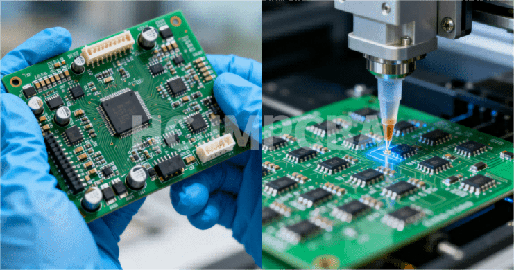
Soldering is the most critical process in PCB assembly. It joins surface-mount and through-hole components to the PCB using solder as the conductive medium. A well-formed solder joint provides both electrical continuity and mechanical strength. A defective joint — even a single one — can render an entire board non-functional or cause intermittent failures that are notoriously difficult to diagnose in the field.
For hardware engineers and procurement teams, understanding soldering defects is not just a technical concern — it is a quality and cost issue. Defects caught at inspection cost pennies to rework. Defects that escape to the field can cost thousands in warranty claims, product recalls, and reputational damage.
At Guangzhou Huachuang Precision Technology Co., Ltd. (HCJMPCBA), we treat soldering quality as a process discipline, not an inspection outcome. With nearly 3,500 m² of ESD‑protected manufacturing space, multiple high-speed SMT lines, and ISO9001 and ISO13485 certifications, our soldering processes are controlled, monitored, and continuously improved to deliver reliable PCBA for industrial, medical, and automation applications.
Common Soldering Defects and Their Effects
Soldering defects can be classified into several categories based on their failure modes. Understanding each type is the first step toward effective prevention and detection.
Open Circuit Defects
Solder Opens occur when there is insufficient connection between a component lead and the PCB pad, leaving the circuit incomplete and preventing current flow. These are typically visible as missing or inadequate solder fillets.
Lifted Pads happen when excessive heat or mechanical stress causes the PCB pad to detach from the substrate, resulting in a permanent loss of connection. This defect is particularly problematic because it often damages the board itself, making repair difficult or impossible.
Solder Skips occur when solder is not applied to the pads of surface-mount devices, leaving areas completely unsoldered with open circuits.
Short Circuit Defects
Solder Bridges form when excess solder creates an unintended connection between adjacent conductors on the PCB. This creates a short circuit that can cause the board to malfunction or fail catastrophically.
Solder Balls are small, stray spheres of solder on the PCB surface. While a single solder ball may not cause immediate failure, they can become dislodged during operation or lodge between conductors, creating intermittent shorts.
Solder Splash refers to unwanted solder droplets caused by impurities or contaminants in the soldering process.
Weak Joint Defects
Cold Solder Joints result from insufficient heat during soldering. They are characterized by a rough, dull, grainy appearance rather than the smooth, shiny surface of a properly formed joint. Cold joints have poor mechanical strength and can crack under thermal or mechanical stress.
Disturbed Joints occur when the joint is moved during the soldering process before the solder has fully solidified. This prevents proper bonding and creates a joint that may pass initial inspection but fail under stress.
Solder Voids are spaces within the solder joint caused by contamination, trapped flux, or inadequate wetting. Voids weaken the mechanical and electrical integrity of the joint and are particularly concerning in power electronics where thermal conductivity is critical.
Insufficient Solder results in a joint with inadequate solder volume, compromising both electrical and mechanical integrity.
Other Defects
Solder Dewetting occurs when solder does not properly adhere to the PCB pad or component lead. The solder may pull back, leaving a thin, irregular coating rather than a proper fillet.
Solder Flux Residue left on the board can cause corrosion or insulation resistance problems over time. While not immediately fatal, residue can lead to reliability issues in high-humidity environments.
Solder Cracking results from mechanical stress or thermal cycling. Cracks degrade both the strength and conductivity of the joint and can lead to intermittent failures.
Tombstoning is a defect where one end of a surface-mount component lifts off the pad during reflow, leaving the component standing on end like a tombstone. This occurs when the wetting forces on the two pads are unbalanced, often due to thermal imbalances or differences in pad sizes.
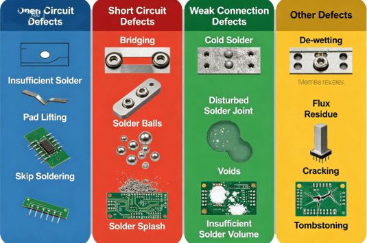
Common Welding Defect Classification Diagram Hcjmpcba
Root Causes of Soldering Defects
Effective prevention requires understanding why defects occur. The root causes generally fall into several categories:
Thermal Issues: Insufficient heat or excessively rapid cooling produces cold joints and voids. Uneven heating across the board leads to tombstoning. Thermal shock from extreme temperature differentials can cause pads to lift and joints to crack.
Solder Quantity: Too much solder produces bridges and solder balls. Insufficient solder yields opens and weak joints.
Contamination: Oils, oxides, or chemicals on component leads, PCB pads, or solder paste can prevent proper wetting and adhesion. Oxidation on surfaces receiving soldering is a common cause of non-wetting.
Component Placement: Incorrect component alignment or placement can result in defects including tombstoning, offset components, and insufficient wetting.
Design Issues: Inadequate thermal relief in pad designs contributes to tombstoning. Poor pad geometry and insufficient spacing between conductors increase the risk of bridges and insufficient wetting.
Solder Paste Quality: Low metal content, improper flux chemistry, or degraded paste can lead to solder balling, bridging, and poor wetting.
Process Parameters: Unstable reflow temperature profiles, inconsistent printing, and suboptimal stencil design all contribute to defect formation.
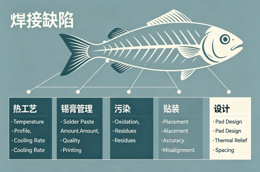
Fishbone Diagram Of The Root Causes Of Welding Defects Hcjmpcba
Inspection Methods for Soldering Defects
Detecting soldering defects requires a multi-layered inspection strategy. No single method catches everything.
Visual Inspection
Manual visual inspection is the most basic method. Trained inspectors examine boards for visible defects — missing components, poor fillets, bridging, and tombstoning. However, visual inspection is subjective, inconsistent, and cannot detect hidden defects like voids or BGA solder joint issues.
AOI systems use high-resolution cameras and image processing software to inspect boards for soldering and component placement defects. They compare each board against CAD data and reference images to detect missing components, misalignment, bridging, and surface-level solder defects.
AOI is fast, repeatable, and suitable for high-volume production. However, AOI cannot see through components — it cannot inspect hidden solder joints under BGAs, QFNs, or other area-array packages.
X-Ray Inspection (AXI)
X-ray inspection uses radiation to penetrate solid objects and capture images of internal structures. It is the only practical method for inspecting hidden solder joints under BGAs, QFNs, and other components with terminations underneath the package.
X-ray can detect voids, cracks, solder bridges, and insufficient solder in hidden joints. It is essential for high-reliability applications where hidden joint defects are unacceptable.
ICT uses a bed-of-nails fixture to make electrical contact with test points on the board. It can identify soldering and component problems — opens, shorts, incorrect component values, and polarity errors. ICT is fast and provides comprehensive electrical verification but cannot detect physical defects like voids or cracks unless they affect electrical parameters.
Functional Testing (FT)
Functional testing powers up the board and verifies that it performs according to specifications. While functional testing catches defects that affect overall board operation, it does not isolate the root cause — a board that fails functional test still requires diagnostic work to identify which solder joint or component is responsible.
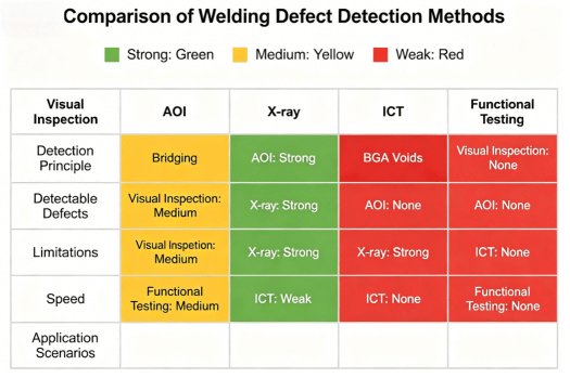
Comparison Table Of Welding Defect Detection Methods Hcjmpcba
Prevention Strategies
Prevention is always more cost-effective than detection and rework. A comprehensive prevention strategy addresses design, materials, process, and inspection.
Design for Soldering Quality
-
Provide adequate spacing between conductors to prevent bridging
-
Design generous thermal relief in pad layouts to avoid tombstoning
-
Ensure component pad sizes match the component footprint
-
Validate designs through prototyping and functional testing
Solder Paste Control
-
Use high-quality solder paste from reputable suppliers
-
Store and handle paste according to manufacturer specifications
-
Verify paste print quality with 3D SPI before component placement
Process Optimization
-
Develop and validate reflow profiles for each board type
-
Monitor and control oven temperature uniformity
-
Implement closed-loop process controls for printing and placement
-
Use nitrogen atmosphere in reflow to improve wetting and reduce voids
Inspection Integration
-
Implement AOI after reflow for surface defect detection
-
Use X-ray inspection for BGAs, QFNs, and power modules
-
Apply ICT for electrical verification
-
Perform functional testing for final validation
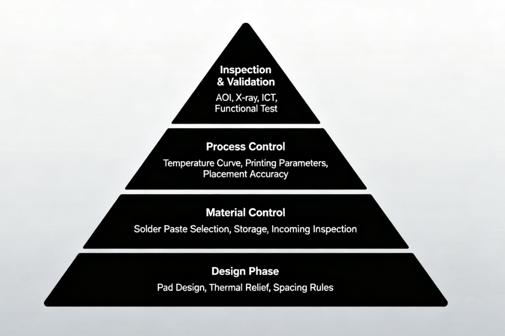
Welding Quality Prevention Strategy Framework Diagram Hcjmpcba
HCJMPCBA: Your Soldering Quality Partner
At Guangzhou Huachuang Precision Technology Co., Ltd. (HCJMPCBA), we understand that soldering quality is not achieved through inspection alone — it is built through disciplined process control at every stage.
Our nearly 3,500 m² ESD‑protected manufacturing facility houses multiple high-speed SMT lines with closed-loop process controls. Our ISO9001 quality management and ISO13485 medical device quality management certifications ensure that every board meets the highest standards of workmanship and reliability.
Our soldering quality capabilities include:
-
Comprehensive inspection — AOI, X-ray, ICT, and functional testing all in-house
-
Process control — 3D SPI for paste verification, closed-loop reflow profiling, and statistical process monitoring
-
Component traceability — Full material history via our intelligent MES system
-
Defect prevention — Engineering support for process parameter development and production readiness reviews
-
Scalable production — From prototypes to mass production of tens of thousands per month, with consistent quality standards
We provide transparent quality reporting with complete traceability documentation — giving procurement teams the audit-ready records they need and hardware engineers the confidence that their designs will be built right.
Guangzhou Huachuang Precision Technology Co., Ltd. (HCJMPCBA) — Your PCBA partner for soldering quality and reliability.