Engineer’s Perspective — Selecting & Applying Circuit Board Components for Performance & Reliability
Introduction – Why Circuit Board Components Define PCB Performance & Supply Chain Value A bare

Chip-on-board (COB) assembly is a packaging method where a bare semiconductor die is mounted directly onto a substrate — typically a PCB — instead of being housed in an individual plastic or ceramic package first. The die is electrically connected to the board and then protected with a layer of encapsulant, most often a black epoxy “glob top,” which is why COB modules are sometimes recognized by that characteristic dome or dot.
Because the packaging step is skipped, COB is often described as a die-level or chip-level assembly technique, distinct from surface mount technology (SMT), which places pre-packaged components (like QFNs or BGAs) onto a board. In conventional SMT, a chip manufacturer packages the die inside a protective housing with its own leads or solder balls, and that finished component is later soldered onto a PCB. COB packaging removes that intermediate step. The unpackaged die — the raw piece of silicon — is attached straight to the board, wired to the circuit, and then encapsulated in place.
At Guangzhou Huachuang Precision Technology Co., Ltd. (HCJMPCBA), we offer COB assembly as part of our comprehensive PCBA services. With nearly 3,500 m² of ESD‑protected manufacturing space, multiple high-speed SMT lines, and ISO9001 quality management and ISO13485 medical device quality management certifications, we provide reliable COB assembly for industrial, medical, and consumer electronics applications.
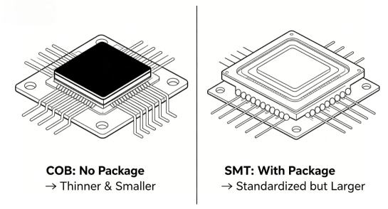
Comparison Diagram Of Cob And Smt Packaging Structures
COB changes several practical aspects of PCB assembly compared to using packaged components:
Footprint — COB modules are typically smaller and thinner, since there is no separate package body. The die is mounted directly on the board, eliminating the extra space required by a plastic or ceramic housing.
Thermal path — With no package material between the die and substrate, heat can dissipate more directly in many designs. This is particularly valuable in power-sensitive applications where junction temperature directly affects reliability and lifetime.
Handling — Bare die are more fragile and sensitive to contamination than packaged parts, so they require controlled handling conditions — including ESD protection, cleanroom environments, and specialized equipment.
Design flexibility — Multiple die can sometimes be placed close together on one substrate, which is useful for compact, multi-chip modules. This enables system integration that would be impossible with individually packaged components.
Because COB merges the component-packaging step and the board-assembly step into one process, it is sometimes referred to in the industry as “level 1.5 packaging” — a step between chip-level packaging and standard board-level assembly.
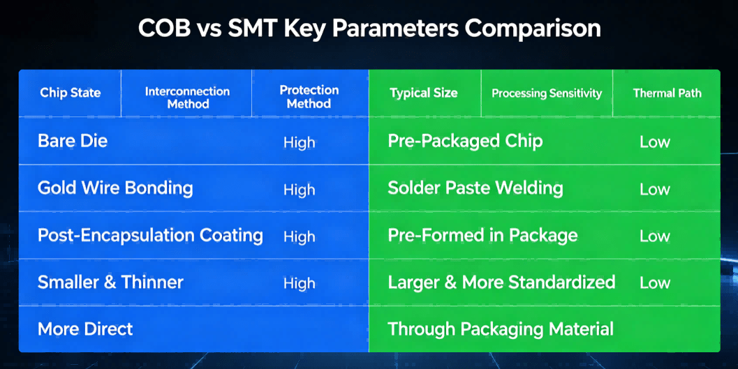
Comparison Table Of Key Parameters Between Cob And Smt
At a high level, COB assembly follows three main stages:
The bare die is bonded to the substrate, usually with an adhesive such as conductive or non-conductive epoxy. This step secures the die mechanically and, depending on the adhesive used, may also establish an electrical or thermal connection to the board.
The die attach process requires precise placement accuracy — typically within ±25 μm — and careful control of adhesive dispensing volume to avoid contamination of bond pads. The adhesive is then cured at controlled temperatures to achieve the required bond strength.
Fine wires — typically gold or aluminum — are used to connect the bond pads on the die to the corresponding pads or traces on the substrate. This replaces the internal wiring that would normally exist inside a packaged component.
Wire bonding is performed using either thermosonic or ultrasonic bonding techniques. Gold wire (typically 0.8–1.0 mil diameter) is most common for its excellent conductivity and corrosion resistance. The wire bonds are formed with precise loop height control to ensure they remain within the encapsulant profile and do not short to adjacent pads.
Once the die and wires are connected, the assembly is covered with a protective encapsulant, commonly a glob-top epoxy. This shields the die and wire bonds from moisture, dust, physical contact, and other environmental factors, since there is no longer a plastic package doing that job.
The result is a functioning circuit where the die, its connections, and its protection are all built up directly on the board rather than assembled beforehand inside a separate package.
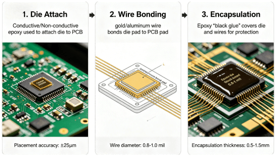
Three Step Process Flow Chart For Cob Assembly
COB assembly shows up most often in applications where size, thickness, or thermal performance matter more than using standardized, pre-packaged parts. Common examples include:
LED Modules — COB LEDs place multiple LED chips on a single substrate under one encapsulant, producing a more uniform light source than individually packaged LEDs. This is widely used in automotive lighting, general illumination, and backlighting applications.
Sensors — Many sensor modules use COB to keep the sensing die as close as possible to the board, reducing size and signal path length. This is critical for optical sensors, pressure sensors, and MEMS devices where parasitic capacitance and signal integrity are concerns.
Wearables — Space-constrained devices benefit from the reduced footprint and thickness that COB allows compared to packaged components. Smartwatches, fitness trackers, and medical patches all leverage COB for miniaturization.
Compact Consumer Modules — Products such as smart cards, small camera modules, and other space-limited electronics use COB to fit more function into less board area.
Medical Devices — Implantable and disposable medical electronics benefit from COB’s small size and the ability to encapsulate the entire assembly for improved reliability in challenging environments.
These are general, widely recognized applications of the technique rather than an exhaustive list — the right approach for any given product depends on its specific electrical, thermal, and mechanical requirements.
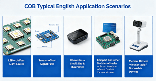
Diagram Of Typical Cob Application Scenarios
| Aspect | Chip on Board (COB) | Standard SMT (Packaged Components) |
|---|---|---|
| Die state | Bare die | Pre-packaged die |
| Connection method | Wire bonding | Solder (leads/balls) |
| Protection | Applied after assembly (encapsulant) | Built into the package beforehand |
| Typical footprint | Smaller, thinner | Larger, standardized |
| Handling sensitivity | Higher (bare die is fragile) | Lower (package protects die) |
In short, COB assembly is a die-level packaging approach built around three steps — die attach, wire bonding, and encapsulation — that trades some of the convenience of pre-packaged components for a smaller footprint and a more direct thermal path.
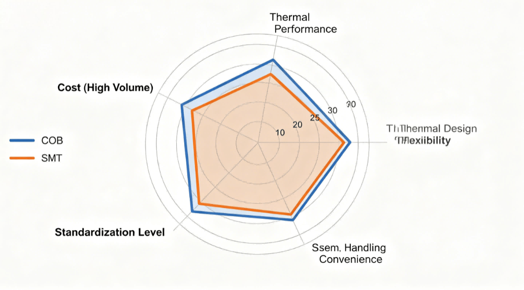
Radar Chart Comparing Advantages And Disadvantages Of Cob And Smt
COB assembly requires stricter process controls than conventional SMT due to the fragility of bare die and the irreversibility of encapsulation.
Cleanroom Environment — Bare die are sensitive to particulate contamination. Our COB assembly is performed in controlled environments with ESD protection and particulate monitoring to maintain cleanliness standards appropriate for die-level processing.
Die Attach Control — Adhesive dispensing volume and placement accuracy are critical. Insufficient adhesive causes weak mechanical bonds; excess adhesive can contaminate bond pads and cause wire bonding failures. Our equipment provides closed-loop control of dispensing parameters.
Wire Bonding Verification — Wire bond strength is verified through pull testing per MIL-STD-883 methods. Bonds must meet minimum pull strength requirements before encapsulation proceeds.
Encapsulation Integrity — The glob-top epoxy must fully cover the die and wire bonds without voids, and the cured encapsulant must pass visual inspection for surface defects and coverage completeness.
Thermal and Environmental Testing — For medical and industrial applications, COB assemblies may undergo thermal cycling, humidity exposure, and other reliability tests to validate performance under end-use conditions.
At HCJMPCBA, our ISO9001 and ISO13485 quality systems provide the framework for these controls. We maintain full traceability of die lots, adhesive batches, and wire materials, and we provide comprehensive documentation with every COB assembly order.
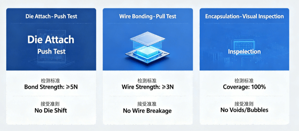
Cob Assembly Quality Control Checkpoint Diagram
One of the challenges with COB assembly is scaling from prototype to production. The same die attach, wire bonding, and encapsulation processes that work for a 10-unit prototype must be repeatable for a 10,000-unit production run.
Our manufacturing infrastructure supports this transition:
Prototype COB — Fast turnaround for design validation, with flexible process parameters
Pilot COB — 50 to 500 units, with full process documentation and first-article inspection
Volume COB Production — Tens of thousands of units per month, with SPC monitoring and consistent quality
The same engineering team, production equipment, and quality system serve all volumes — so the process that validates your prototype is the same process that delivers your production boards.
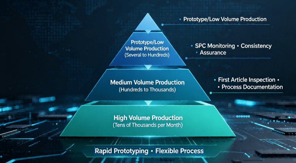
Expansion Diagram Of Cob From Prototype To Mass Production
At Guangzhou Huachuang Precision Technology Co., Ltd. (HCJMPCBA), we offer COB assembly as an integrated part of our full-service PCBA capabilities. Our nearly 3,500 m² ESD‑protected facility, multiple high-speed SMT lines, and ISO9001 and ISO13485 certifications provide the foundation for reliable, high-quality COB assembly.
Our COB capabilities include:
Die attach — Precision epoxy dispensing and placement for bare die
Wire bonding — Gold and aluminum wire bonding for die-to-board interconnection
Encapsulation — Glob-top epoxy protection with controlled cure profiles
Full traceability — Die lot, adhesive batch, and wire material tracking via MES
Quality documentation — Comprehensive test reports and certificates with every order
Scalable production — From prototypes to mass production with consistent quality
We maintain transparent quality reporting with complete traceability documentation — giving hardware engineers confidence that their bare die designs will be built right, and procurement teams the audit-ready records they need.
Introduction – Why Circuit Board Components Define PCB Performance & Supply Chain Value A bare

A clear, detailed guide to the current divider concept and current divider formula. Learn how curren
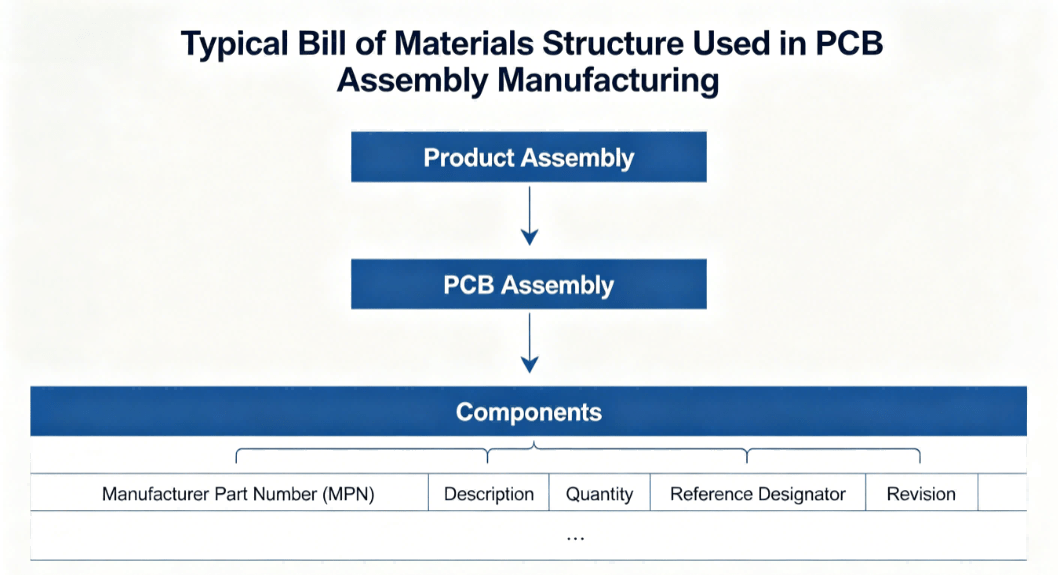
Learn what a Bill of Materials (BOM) is and how to build a BOM for PCB and PCBA manufacturing. This