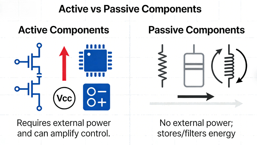
12 Key Differences Between Active and Passive Components: A Complete Guide for PCBA Professionals
Understanding the difference between active and passive components is foundational for reliable PCBA
Conformal Coating Strategies for Industrial IoT Gateway PCBA
Table of Contents
ToggleIndustrial IoT gateways are fundamentally different from consumer‑grade network devices. They are typically installed in outdoor cabinets without temperature control, on factory floors with high dust and vibration, or at remote edge sites where maintenance access is limited. These unforgiving operating conditions expose bare printed circuit board assemblies to four major destructive factors: extreme temperature cycling from –40°C to +85°C, high humidity leading to condensation, salt spray corrosion in coastal or chemical environments, and continuous mechanical vibration from nearby machinery.
Without professional conformal coating protection, the board surface and solder joints undergo gradual degradation. Oxidation of pads, micro‑short circuits caused by moisture bridging, and fatigue of component terminations under thermal stress become the primary failure mechanisms. Field reliability data from large‑scale IoT gateway deployments show that uncoated PCBA in standard industrial environments achieves an average MTBF of only about 18 months. In contrast, assemblies that receive an optimized coating process can extend MTBF to over 60 months, meeting the rigorous uptime requirements of edge computing and industrial automation.
At Guangzhou Huachuang Precision Technology Co., Ltd. (HCJMPCBA), we specialize in high‑reliability PCBA manufacturing. With nearly 3,500 m² of ESD‑protected workshops and multiple high‑speed SMT lines, we have accumulated extensive experience in conformal coating for industrial control, medical equipment, and intelligent manufacturing. The following strategies are drawn from our daily practice and are tailored specifically for industrial IoT gateway applications.
Choosing the right coating material is the foundation of reliability. The material directly affects moisture resistance, signal integrity, reworkability, and environmental adaptability. Among the four mainstream coating materials – acrylic (AR), polyurethane (UR), silicone (SR), and epoxy (ER) – each shows distinct performance differences in edge‑gateway scenarios, particularly in moisture vapour transmission rate, rework difficulty, and attenuation of millimetre‑wave RF signals.
For industrial IoT gateways that increasingly integrate millimetre‑wave communication modules, the coating must balance corrosion protection with minimal dielectric interference. Based on comprehensive performance data, acrylic and polyurethane emerge as the optimal choices for most gateway designs. They provide robust protection against condensation and corrosion while causing negligible signal attenuation at high frequencies, ensuring stable data transmission for edge communication. Silicone, though excellent in vibration damping, introduces slight interference with millimetre‑wave signals and is therefore recommended only for non‑RF areas. Epoxy, despite superior moisture barrier properties, is nearly impossible to rework and significantly attenuates high‑frequency signals, making it unsuitable for gateway core boards.
In our PCBA contract manufacturing service, we always evaluate the actual deployment environment and signal requirements of each product before recommending a specific coating material. This tailored approach ensures that protection and signal integrity are both achieved.
Even with the best material, improper application can compromise performance and introduce new failure modes. Traditional full‑board spray coating has notable drawbacks for precision IoT gateway boards: it cannot selectively mask connectors, heat sinks, test points, and RF antenna no‑spray zones. This often leads to poor contact in connectors, blocked heat dissipation paths, and detuned antenna performance.
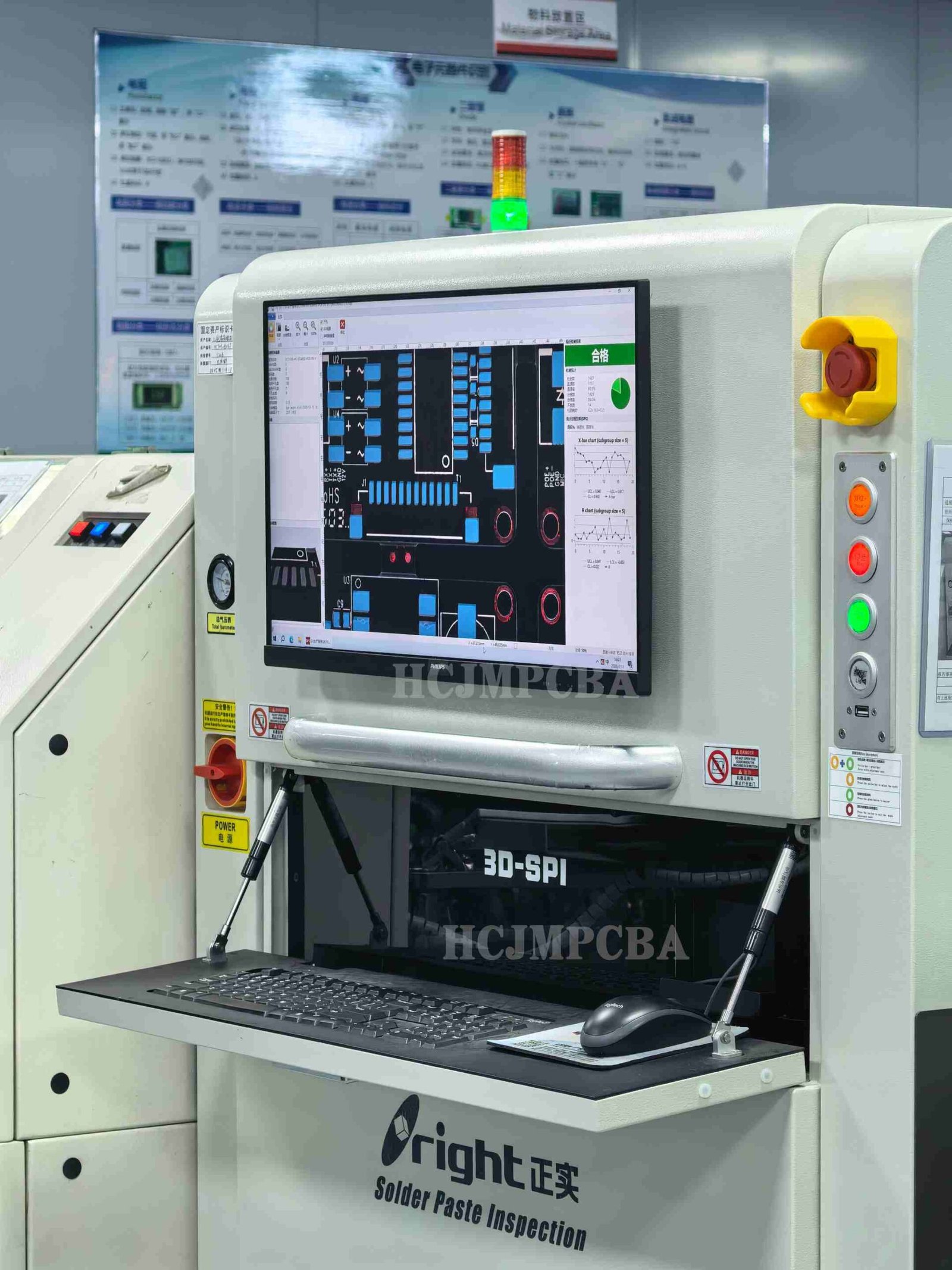
Selective coating solves these issues through programmable positioning and metered deposition. At HCJMPCBA, we use high‑precision selective coating equipment with positioning accuracy of ±0.1 mm. This non‑contact jetting method eliminates the risk of contaminating dense fine‑pitch pads and antenna lands. Compared with conventional spraying, selective coating reduces material waste by approximately 35% while ensuring that critical areas – component leads and solder joints – receive full, uniform coverage.
In addition to precise application, customised masking is essential to protect functional zones. We develop dedicated high‑temperature fixtures for each gateway board design, covering external connectors, functional test pads, and thermal openings before coating. After coating and full curing, these fixtures are removed cleanly without leaving adhesive residue, preserving electrical connectivity and thermal performance.
Precise application must be paired with standardised inspection to guarantee long‑term field reliability. All our conformal coating processes for industrial IoT gateway PCBA strictly follow IPC‑CC‑830B acceptance criteria, with quantified specifications for coating thickness, defect classification, and batch validation.
For the most widely used acrylic coatings on gateway boards, we control the dry‑film thickness within 25–75 μm. Thinner films fail to form a complete protective barrier, while thicker films are prone to cracking under thermal cycling and can impede component heat dissipation. Regarding defects, IPC‑CC‑830B clearly defines unacceptable conditions: bubbles larger than 0.5 mm, pinholes in high‑density circuit areas, and local skips on solder joints and component edges.
For batch quality verification, we employ 365 nm UV fluorescence inspection – the coating material exhibits clear fluorescence under UV light, allowing rapid visual verification of entire‑board coverage and identification of micro‑scopic missed areas that are invisible to the naked eye. To ensure process consistency across multiple batches, our intelligent MES system provides UID‑level component traceability. All critical coating parameters – including thickness, curing temperature, and process duration – are recorded in real time, enabling complete lifecycle traceability for every gateway board we produce.
The multi‑variety, small‑batch nature of industrial IoT gateway manufacturing inevitably requires targeted rework and secondary coating during prototype iterations and field repairs. Improper rework often leads to delamination, residual contamination, or reduced adhesion, all of which compromise long‑term reliability in harsh environments.
To address this, we apply two differentiated coating removal methods depending on the board scenario. For precision RF modules and fine‑pitch components with local coating defects, we use hot‑air local removal with temperature controlled between 120°C and 150°C to avoid thermal damage to sensitive components. For non‑precision areas with extensive ineffective coating, we adopt chemical solvent removal, which improves efficiency while ensuring no corrosive residues remain on the board surface.
After defect removal and professional surface activation cleaning, secondary conformal coating can be properly applied. Since reworked surfaces differ from the original virgin substrate, adhesion performance becomes the key indicator. We strictly perform cross‑cut adhesion testing per ISO 2409, accepting only boards that achieve Grade 0–1 (no peeling or edge lifting). This standardised validation effectively prevents coating delamination and failure during extended field operation.
Coating reliability depends not only on manufacturing execution but also on front‑end PCB design for manufacturability (DFM). Poor board layout creates un‑coat‑able dead corners, hidden contamination risks, or signal degradation that cannot be fully compensated by subsequent processes.
Based on our years of experience in industrial IoT PCBA manufacturing and coating, we have summarised three DFM rules specifically for harsh‑environment gateway boards:
Connector edge clearance: Reserve at least 2 mm of clearance between external connectors and peripheral circuits. This prevents coating material from seeping into connector pins during selective coating, ensuring stable insertion and long‑term contact reliability.
Thermal opening optimisation: Define the dimensions and edge recess of thermal openings clearly in the design, and mark separate masking areas in the fabrication drawings to prevent coating from clogging heat‑dissipation paths, avoiding overheating of power components under high‑temperature operation.
Antenna no‑spray marking: Explicitly designate no‑spray zones for millimetre‑wave antennas and RF circuits on the PCB artwork, and set corresponding prohibited areas in the process system. This fundamentally eliminates high‑frequency signal attenuation risks.
By incorporating these DFM guidelines early in the design phase, engineers can significantly improve coating yield and reduce field failure rates.
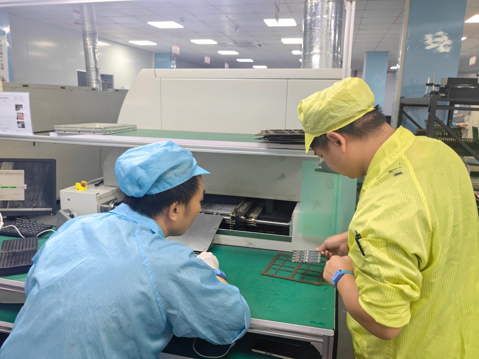
For many hardware engineers and procurement professionals, the ability to scale from prototype to high‑volume production without compromising quality is a critical concern. At HCJMPCBA, our manufacturing infrastructure is built for both flexibility and capacity. Our facility houses multiple high‑speed SMT lines, automated optical inspection (AOI), X‑ray inspection, and the selective coating equipment mentioned above – all integrated with our MES system for real‑time process control.
Our production capacity supports volumes ranging from pilot runs of a few hundred boards to mass production of tens of thousands per month. We maintain strict process controls and regular calibration to ensure that the same coating quality achieved during NPI is consistently delivered in volume batches. Our supply chain team works closely with coating material suppliers to guarantee stable raw material availability, while our engineering staff provides on‑site DFM reviews and process optimisation support to help customers shorten time‑to‑market.
We also understand that cost efficiency matters. Our selective coating process reduces material waste and rework rates, directly lowering the total cost of ownership for our customers. With transparent quality reporting and full traceability, we offer procurement teams the confidence that every board meets the required specifications.
Most field failures of industrial IoT gateway boards in harsh environments stem not from component defects but from mismatched coating materials, un‑optimised application processes, or poor PCB layout. These are issues that can be addressed with the right expertise and manufacturing partnership.
Our engineering team at HCJMPCBA has a proven track record in high‑reliability industrial control and edge‑communication PCBA. We offer one‑stop manufacturing services including DFM review, material selection, sample prototyping, and volume production. If you are developing or mass‑producing industrial IoT gateway boards and need assistance with conformal coating strategy, we invite you to contact our process engineering team for a no‑obligation consultation.
We provide customised recommendations based on your specific environmental conditions, signal requirements, and production schedules. Let us help you achieve the MTBF and field reliability that your end customers demand – from the first prototype to the millionth unit.
Understanding the difference between active and passive components is foundational for reliable PCBA
Learn how to clean battery corrosion in remote control devices and other electronics with safe, step
Learn 5 powerful customer communication strategies that position HCJMPCBA as one of the best PCB man