10 Critical Steps to Mastering HDI PCB Design and High-Density Mass Production Reliability
Master hdi pcb design and high-density interconnect manufacturing with this engineering guide. Learn
This guide is maintained by the HCJMPCBA engineering team and updated with production checklists to ensure substrate-process compatibility. Copper Clad Laminate (CCL) is the backbone of any PCB, determining thermal stability and signal integrity. With the industry shift toward lead free soldering, selecting a CCL that can withstand the higher lead free solder melting point (typically 217°C) without delamination is critical. Our manufacturing protocols utilize IPC-4101E standards to validate every batch before mass PCBA production.
Thermal Window: The gap between lead free solder melting point and CCL thermal decomposition (Td) is narrower than in leaded processes, requiring higher-tier materials (Mid-to-High Tg).
Mechanical Stress: Lead free solder for electronics requires higher peak reflow temperatures, increasing the risk of Z-axis expansion and PTH (Plating Through Hole) failure.
Risk Mitigation: Quality assurance depends on requesting raw data and traceability (lot/batch) for the raw CCL to prevent latent field failures.
Understanding the transition from leaded vs lead free solder is fundamental for any PCBA project. The primary driver of material selection is the thermal profile.
Traditional lead solder vs lead free solder comparisons center on the melting point of lead solder, which is a reliable 183°C. In contrast, the lead free solder melting point for the industry-standard SAC305 alloy is approximately 217°C. When considering the melting temperature lead free solder requires for a full liquidus state during reflow, engineers must calibrate ovens to reach peak temperatures of 245°C to 260°C.
This 30°C–40°C increase in lead free soldering temperature places immense pressure on the PCB substrate. If the non lead solder process is applied to a low-grade CCL, the resin system may reach its melting point for lead free solder compatibility limits, leading to “popcorning” or internal layer separation.
To answer “what is copper clad laminate and how to do it” correctly, one must look at the composite nature of the material. A CCL consists of copper foil, reinforced fiberglass cloth, and an epoxy resin system.
The composition of lead free solder (often Tin, Silver, and Copper) dictates that the CCL must have a high Td (Decomposition Temperature). While a user might ask “what is lead-free solder made of,” a savvy engineer asks, “Is the CCL resin chemistry compatible with the flux chemistry of my lead-free solder alloy?”
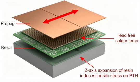
Copper Clad Laminate Layer Structure And Thermal Stress Interaction
Choosing the right material is a balance of cost and reliability. Use this table to align your lead free solder temperature needs with the correct CCL grade.
| CCL Category | Tg (Glass Transition) | Td (Decomposition) | Lead-Free Compatibility | Best Use Case |
| Standard FR-4 | 130°C – 140°C | < 310°C | Marginal / Risk of Delamination | Consumer toys, low-complexity disposables |
| Mid-Tg FR-4 | 150°C – 160°C | 325°C+ | Good (HCJMPCBA Standard) | Industrial controls, LED drivers, IoT |
| High-Tg FR-4 | 170°C – 180°C | 340°C+ | Excellent | Server boards, Automotive, AI Hardware |
| Halogen-Free | 150°C – 170°C | 350°C+ | High Reliability | Green electronics, high-density PCBA |
At HCJMPCBA, we don’t just “buy and build.” We follow a rigorous 5-step engineering verification to ensure your lead free solder for electronics remains reliable over the product’s lifespan.
Material Verification via Method Number + Revision: Every batch of CCL is verified against IPC-4101E specifications. We check the specific lead free solder vs lead solder thermal resistance ratings provided by the laminate manufacturer.
Design of the Sample Plan: For new PCBA designs, we implement a sample plan involving thermal shock testing (typically 3 to 6 reflow cycles) to ensure the substrate doesn’t blister.
Strict Test Conditions: We simulate the actual melting temperature of lead free solder reflow profile in our labs, focusing on the “Time Above Liquidus” (TAL) to ensure the CCL resin doesn’t degrade.
Raw Data Extraction: We record the raw data from AOI (Automated Optical Inspection) and X-Ray post-soldering to detect any micro-voiding or delamination that is invisible to the naked eye.
Full Traceability Implementation: Every board is tied to a traceability (lot/batch/serial) system. If a substrate defect is found, we can trace it back to the specific CCL batch and the lead free solder temp settings used during that production hour.
When you audit a PCBA factory, look for these specific verification markers:
| Verification Metric | Reference Standard | HCJMPCBA Internal Requirement | Evidence Provided |
| Thermal Stress Test | IPC-TM-650 2.6.8 | 288°C for 10 seconds, 3 cycles | Micro-section Raw Data |
| Solderability | IPC-J-STD-003 | >95% coverage with lead free solder | Wetting Balance Curves |
| Cleanliness | IPC-TM-650 2.3.25 | < 1.56 μg/cm² NaCl equivalent | Ionic Contamination Report |
| Peel Strength | IPC-4101 | > 1.1 N/mm after thermal shock | Material Test Certificate |
Include the following in your RFQ or Quality Agreement to protect your project:
“All PCBA substrates must utilize CCL materials compliant with IPC-4101E, verified for lead-free solder vs lead compatibility. The Manufacturer shall provide a Certificate of Conformance (CoC) including lot/batch traceability, and must maintain raw data for thermal stress tests (Method 2.6.8) for a minimum of 2 years. Maximum peak lead free solder temperature during reflow must not exceed 260°C.”
Ignoring the Td (Decomposition Temperature): Many focus on Tg, but Td is more critical for surviving the melting point of soldering lead-free alternatives. High Td prevents resin breakdown.
Using “Lead-Era” Laminates: Old-stock FR-4 designed for lead vs lead free solder (183°C peak) will often fail during the second side reflow of a modern lead-free soldering process.
Overlooking CTE (Coefficient of Thermal Expansion): As lead free solder temp rises, the Z-axis expansion increases. Mismatched CTE leads to cracked copper barrels in vias.
Inconsistent Solder Mask Selection: High lead free soldering temperature can cause low-quality solder masks to discolor or lose adhesion to the CCL.
Neglecting Traceability: Without traceability (lot/batch/serial), if a board fails in the field, you cannot determine if it was a material defect or a process deviation.
Consider an Automotive AI Controller or an Industrial Power Supply. These devices operate in high-vibration and high-heat environments. Using a standard FR-4 might seem cost-effective during the PCB design phase. However, when subjected to the melting temperature lead free solder demands during assembly, and the subsequent thermal cycling of the engine bay, a standard CCL will suffer from “pad cratering.” HCJMPCBA recommends High-Tg, low-CTE materials for these “Mission Critical” families of products.
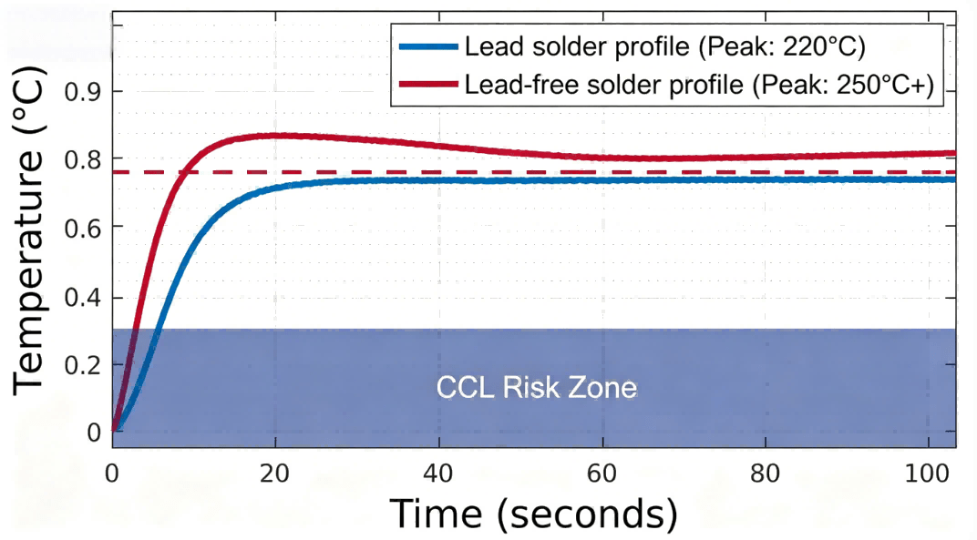
Reflow Soldering Temperature Profile Comparing Lead Vs Lead Free Solder
Q: Is lead free solder better for the environment but worse for the PCB? A: Is lead free solder better? Environmentally, yes (RoHS compliance). However, technically, it is more “aggressive” toward the PCB. The higher lead free soldering temperature requires more resilient CCL materials to prevent substrate warping.
Q: What is lead free soldering’s biggest impact on cost? A: Beyond the lead free solder alloy cost, the primary expense is the requirement for better-performing CCL (Mid/High Tg) and more precise thermal management in the PCBA oven.
Q: Can I use leaded solder on a lead-free rated CCL? A: Yes. A PCB designed for the high melting temperature of lead free solder can easily handle the lower temperatures of leaded solder. However, the reverse is not true.
Q: How do I know the melting temperature lead free solder is actually reaching in your factory? A: At HCJMPCBA, we use KIC profile testers to generate a thermal map of the board. This raw data is available for client review to prove the temp for lead free solder was maintained within the ±5°C window.
Q: Does lead free solder composition affect signal integrity? A: The solder itself has a minor impact, but the CCL used to survive the lead-free solder melting point (like high-speed, low-loss laminates) has a massive impact on signal performance.
When partnering with us for mass production, you have full access to:
Incoming Inspection Reports: CCL lot/batch verification and IPC-4101 CoC.
Reflow Profiles: Real-time test conditions and temp for lead free solder logs for your specific PCBA.
Traceability Data: Linkage between the serial number on your board and the raw material batch.
Cross-Section Analysis: Visual proof of interlaminate bonding and PTH integrity after lead free soldering.
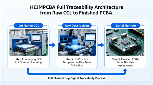
Hcjmpcba Full Traceability Architecture From Raw Ccl To Finished Pcba
For more information about PCBA services, please contact Guangzhou Huachuang Precision Technology(HCJMPCBA).
Update triggers: standard revision changes / recurring questions / production checklist updates.
Master hdi pcb design and high-density interconnect manufacturing with this engineering guide. Learn
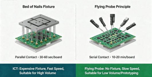
ICT and flying probe testing serve different production phases and volumes. Guangzhou Huachuang Pr
This guide explains how to import component in altium in a production-ready way—so imported parts