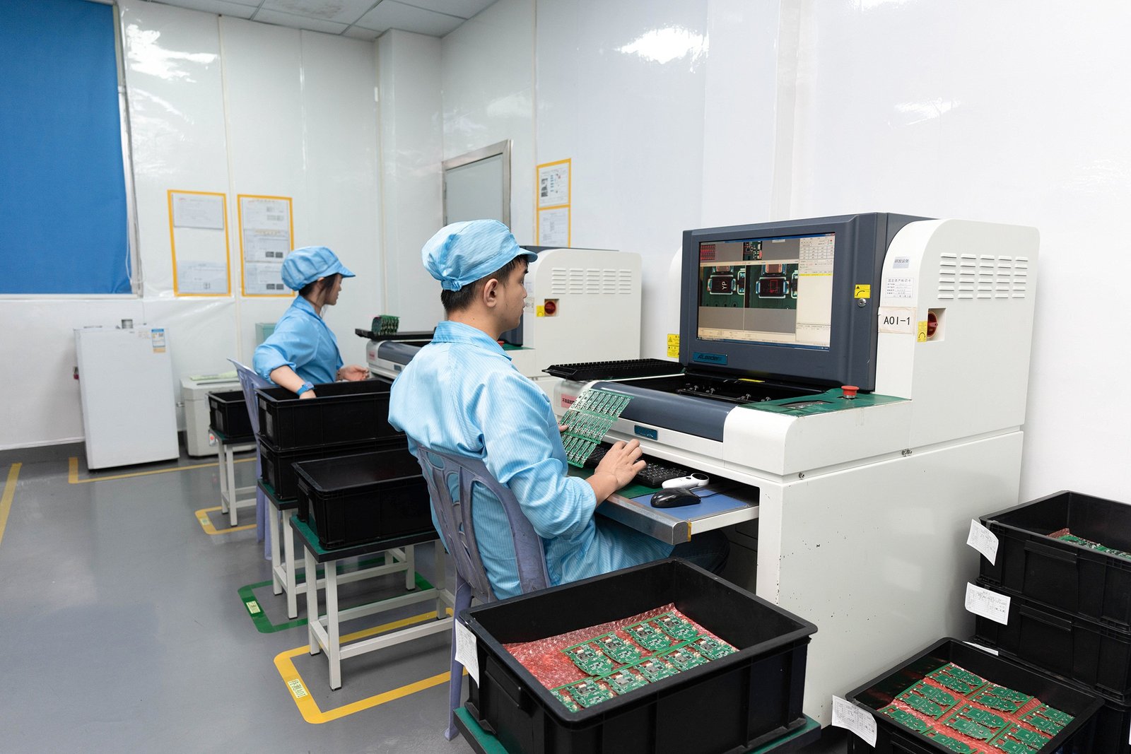
AOI Inspection PCB: 7 Powerful Insights into Automated Optical Inspection in PCB Manufacturing
Automated Optical Inspection (aoi inspection pcb) is a non-contact, high-speed quality control metho
For hardware engineers and electronics procurement professionals, receiving a new batch of bare printed circuit boards (PCBs) is a critical milestone in the product development cycle. However, a board that looks fine at a casual glance can still harbor visual defects that disrupt automated Surface Mount Technology (SMT) assembly lines, lower your production yield, or cause premature field failures.
While internal trace continuity is verified via electrical testing (E-test), structural and surface defects require careful physical inspection. At Guangzhou Huachuang Precision Technology Co., Ltd. (HCJMPCBA), our manufacturing and quality control workflows are built on international standards, specifically IPC-A-600 and IPC-6012 Class 2 (Dedicated Service Electronic Products).
To help your team identify visual anomalies during incoming quality control (IQC), this technical guide breaks down dimensional tolerances, warpage thresholds, and the critical visual defects you must look for before committing your boards to assembly.
Physical dimensions dictate how seamlessly a PCB fits into its mechanical enclosure and how safely it behaves during automated panel de-routing.
Outline Dimensions: Standard FR4 routing should maintain a strict mechanical profile tolerance of $\pm$0.15 mm. For high-precision or automotive applications, this can be tightened to a $\pm$0.10 mm precision milling standard.
V-Cut (V-Score) Depth: The remaining web thickness (the uncut material holding the panel together) must be kept at precisely one-third of the total board thickness. The allowed tolerance for both depth and positional alignment is $\pm$0.10 mm.
V-Cut Blade Alignment: The offset between the top and bottom V-groove scoring blades must not exceed 0.10 mm. Misalignment causes uneven stress distribution when separating the boards, which can rip copper traces or crack solder joints near the board edge.
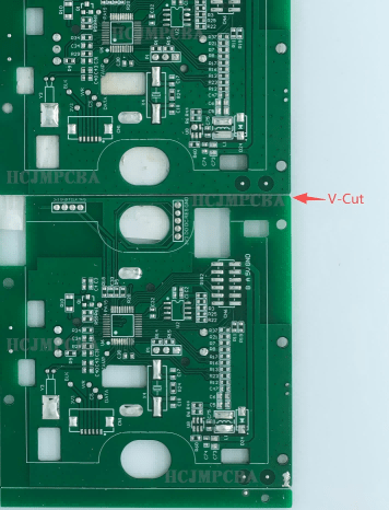
V Cut
Board warpage is an assembly killer. If a board does not sit perfectly flat on the SMT conveyor, solder paste printing becomes uneven, components shift during placement, and complex devices like Ball Grid Arrays (BGAs) suffer from open circuits or head-in-pillow (HIP) solder defects.
To prevent these placement errors, IPC standards classify acceptable warpage based on the component type:
Boards with Surface Mount (SMT) Components: The maximum allowable bow or twist is 0.75% or less. This applies to any board hosting 0402 passives, fine-pitch QFPs, or BGAs.
Boards with Thru-Hole (DIP) Components Only: If the design contains no surface-mount parts, the warpage limit can ease to 1.5% or less.
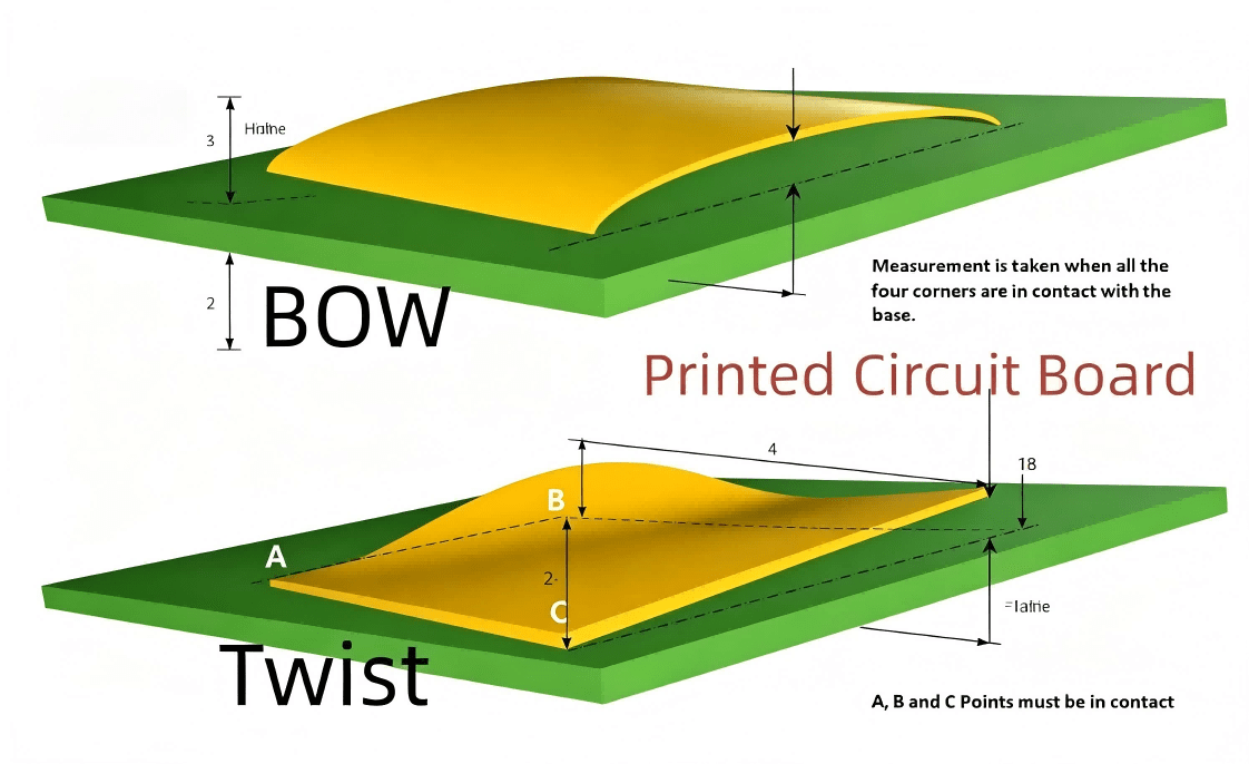
Three-dimensional comparison of PCB bow and twist
Bow: (The maximum perpendicular clearance from a flat surface / Length of the longest board edge) * 100
Twist: (The height of the one corner that lifts off the surface / Diagonal length of the board) * 100
Note: True measurement requires placing the unpopulated PCB on a calibrated precision marble surface plate and performing a four-point pressure test using an inspection feeler gauge.
Solder mask is your primary insulation layer. It prevents unintended solder bridging, protects copper traces from environmental oxidation, and controls the flow of molten alloy.
Mask Height Profiles: The thickness of the solder mask or legend ink encroaching near a pad or via land must not protrude more than 50 microns above the copper level.
The Risk of High Protrusions: If mask ink accumulates too high near a component footprint, small chips or high-density ICs will tilt or “teeter-totter” during placement, leading to tombstoning or open solder joints. Conversely, an insufficient mask layer leads to exposed copper, risking electrical shorts.
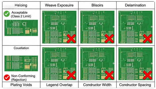
Ipc Class 2 Common Pcb Appearance Defects Identification
Haloing is the localized fracturing or white-shattering pattern seen around drilled holes or routed slots. It occurs when mechanical shearing stresses separate the internal glass fiber layers from the surrounding resin matrix.
Class 2 Borderline: Haloing is acceptable only if the white penetration does not encroach across more than 50% of the distance between the hole edge and the nearest active conductor. Anything beyond that can spread under thermal stress, creating a path for moisture and dendritic growth.
This defect occurs when the protective resin layer over the fiberglass substrate is too thin, leaving the woven fiberglass pattern distinctly visible or exposed to the air.
Class 2 Borderline: Light, localized weave patterns are acceptable if they do not expose raw copper or open the fiberglass bundle. Large, continuous patches of exposed weave are grounds for rejection because they degrade the dielectric breakdown voltage of the laminate.
Blistering occurs when trapped moisture, air, or organic surface contaminants expand under the mask layer during the curing cycle.
Class 2 Borderline: Single isolated bubbles are acceptable if they do not bridge adjacent tracks. Any mask bubble or void exceeding 0.30 mm in diameter, or clusters of blisters running along a trace, are strictly non-conforming. They can pop during the high temperatures of reflow, capturing moisture and causing corrosion.
Delamination is an absolute separation of internal layers or a separation of the outer copper foil from the underlying fiberglass core.
Class 2 Borderline: Zero tolerance. Any visible internal delamination or copper foil blistering means the board is defective. Such boards will catastrophicly delaminate or “popcorn” when subjected to lead-free reflow oven profiles.
A plating void is a localized absence of copper inside the barrel of a plated through-hole, usually caused by air bubbles trapped in the chemistry tanks during the copper deposition phase.
Class 2 Borderline: A single void is acceptable only if it accounts for less than 5% of the total hole barrel length, and no more than 5% of the holes on the board exhibit this issue. Large-scale voids interrupt current flow and thermal dissipation, leading to circuit failures.
Silkscreen markings—such as component designators, polarity markers, logos, and trace barcodes—must be legible and stable.
Class 2 Borderline: Characters must be readable by eye or automated assembly cameras. The primary failure rule: No legend ink is permitted to overlap onto an active, solderable SMD pad surface, as this disrupts solder wetting.
Chemical over-etching or under-etching changes the cross-sectional geometry of your copper traces, directly shifting the trace impedance.
Class 2 Borderline: Outer layer trace widths must stay within $\pm$0.03 mm of the Gerber file dimensions; inner layers must stay within $\pm$0.05 mm. Traces that are too narrow face localized heating and current bottlenecks.
This happens when copper remnants decrease the air gap between two separate nets.
Class 2 Borderline: The remaining space between conductors must not fall below 90% of the minimum clearance specified in your design files. This rule is heavily enforced on industrial control and high-voltage power supply layouts to avoid electrical arcing or leakage currents.
Even a board that achieves perfect visual scores at the end of the factory line can arrive damaged if the packaging is inadequate. To prevent oxidation and handling wear during transit and storage, finished batches require cleanroom-level packaging:
Hermetic Vacuum Packing: Boards are sealed in heavy-gauge ESD moisture barrier bags containing active desiccant pouches and a calibrated humidity indicator card (HIC).
Interleaved Protective Padding: Custom foam inserts or bubble sheets are placed between separate arrays to eliminate friction that could scratch the solder mask or scrape gold/tin plating finishes.
Climate-Controlled Storage: Warehouses should keep conditions steady at 40% to 60% relative humidity and a stable room temperature, preventing any early oxidation on surface finishes like Electroless Nickel Immersion Gold (ENIG) or Immersion Silver.
Q1: Can a standard electrical test (E-test) catch these visual defects?
No. An E-test (whether via flying probe or automated fixture) only checks for direct short circuits or open connections. It cannot detect structural or reliability issues like solder mask blisters, edge haloing, minor trace width reductions, or out-of-spec board warpage, all of which cause failures down the road.
Q2: Why is the 0.75% warpage limit so strictly enforced for SMT boards?
Modern automated pick-and-place systems rely on flat surfaces to drop fine-pitch components (like 0201s or 0.4mm-pitch BGAs) accurately onto solder paste deposits. If a board warps beyond 0.75%, the mechanical offset causes pins to miss the pads or bridge across adjacent paste deposits during reflow.
Q3: What should a procurement manager do if incoming boards show minor weave exposure?
Check the location. If it is a small, isolated area away from high-speed digital lines or high-voltage routing, it falls within IPC Class 2 acceptable limits. However, if the weave exposure is continuous, deep, or touches bare copper tracks, it compromises moisture resistance and should be flagged for rework.
Establishing transparent visual standards gives hardware engineers and procurement managers a clear baseline for evaluating incoming hardware. When your manufacturing partner operates with these exact metrics in mind, it simplifies the transition from prototype validation to volume production.
Operating from our modern facility in the Pacific Industrial Zone, Xintang Town, Zengcheng District, Guangzhou Huachuang Precision Technology Co., Ltd. (HCJMPCBA) combines rigid process control with extensive technical expertise. Every project we handle undergoes automated optical inspection (AOI), laser warpage validation, and dedicated visual reviews to ensure compliance with IPC Class 2 or Class 3 parameters. By keeping our quality expectations aligned with international standards, we help you eliminate assembly risks and deliver robust, reliable electronics to the market.
Looking to verify your next design against production realities? Send your Gerber data and engineering requirements to the team at HCJMPCBA for a thorough DFM analysis and production estimate.
Automated Optical Inspection (aoi inspection pcb) is a non-contact, high-speed quality control metho
Guangzhou Huachuang Precision Technology Co., Ltd. is a leading PCBA manufacturer offering high-qual

Discover what attenuation means in PCB signal transmission—why signal loss matters, what causes it