Guangzhou Huachuang Precision Technology Co., Ltd. – Your Go-To Partner for High-Quality PCBA Solutions
Guangzhou Huachuang Precision Technology Co., Ltd. is a leading PCBA manufacturer offering high-qual
To deploy an effective board-level shield, it helps to understand how a conductive barrier interacts with radiated electromagnetic waves. When a stray electromagnetic wave meets a metallic shield, its attenuation is determined by three main mechanisms:
Reflection: The difference in impedance between free space and a highly conductive metal shield (such as copper, aluminum, or tin-plated steel) causes a large portion of the incident wave’s energy to reflect off the shield’s outer boundary. This mechanism is highly effective against low-frequency electric fields.
Absorption: Electromagnetic wave energy that penetrates the surface of the shield is converted into heat through resistive losses. The effectiveness of this absorption depends on the metal’s thickness, electrical conductivity, and magnetic permeability. High-permeability materials excel at absorbing lower-frequency magnetic noise.
Grounding Interconnection: A metal shield cannot function effectively without a low-impedance connection to the system ground plane. An ungrounded shield can act as a patch antenna, radiating EMI throughout the enclosure. Secure mechanical grounding through a grid of stitching vias converts potential stray fields into harmless return currents.
Engineers can implement EMI shielding at different structural levels depending on the frequency spectrum, weight limits, and product profile.
Stamped metal enclosures made of tin-plated steel, copper, or nickel-silver provide a reliable method to isolate RF circuits and switching regulators. They offer between 40 dB and 80 dB of RF attenuation. These cans can either be soldered directly to a dedicated ground trace pad or snapped into surface-mounted clips for easier rework during debugging.
For internal layers, solid copper pours connected to the system ground act as integrated planar shields. Running grounded guard traces—copper tracks placed alongside critical high-speed lines—helps contain lateral fringing fields and isolates adjacent signal lines from cross-talk.
For thin-profile or weight-sensitive enclosures (such as handheld medical devices or aerospace modules), lightweight conductive paints or silver/nickel-filled polymer coatings can be sprayed directly onto the internal plastic housing to create a protective barrier.
A well-planned multi-layer stackup can minimize the need for heavy external metal shielding. Routing high-speed traces directly adjacent to an uninterrupted reference ground plane helps keep the return path loop area small, minimizing loop inductance and reducing radiated emissions at the board level.
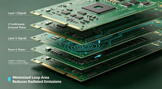
Pcb Multilayer Stackup And Emi Shielding
In a standard 6-layer EMC-optimized configuration, alternating layers—such as Signal-Ground-Signal-Power-Ground-Signal—ensure that every high-speed internal route is sandwiched between reference planes. This configuration minimizes layer-to-layer noise coupling and provides consistent characteristic impedance across the traces.
High-frequency signals are treated as transmission lines where physical layout geometry dictates performance. Maintaining waveform integrity requires strict adherence to three critical DFM layout guidelines:
To control parallel capacitive and inductive coupling between adjacent copper lines, the center-to-center distance between high-speed tracks should be at least three times the width of a single trace ($3W$). This spacing layout limits mutual trace coupling and prevents adjacent digital bit-streams from corrupting nearby signals.
Sharp $90^\circ$ trace corners introduce localized changes in trace width, creating capacitance spikes and impedance mismatches that cause signal reflections. Utilizing smooth $45^\circ$ entry angles or radiused curves helps maintain a consistent transmission line cross-section.
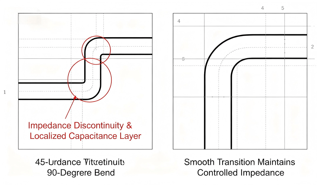
Comparison Of The Influence Of Trace Geometric Angles On Signal Reflection
When a high-speed signal transitions from a top layer to an internal layer through a plated through-hole via, the remaining unused length of the copper barrel forms a “via stub.” At higher frequencies, this stub acts as an open-ended resonant transmission line that reflections energy back into the channel. Utilizing precise depth-controlled backdrilling removes this unused copper, eliminating resonances and helping to open up closed signal eye diagrams.
While a metal shielding can may solve an EMC simulation challenge, it can introduce real-world assembly complexities on a high-throughput automated surface mount technology (SMT) production line. Advanced manufacturing engineering must account for these production realities:
Thermal Shielding Challenges: A large metal shielding can acts as a heat sink inside a convection reflow oven. It blocks radiant infrared heat and redirects hot air currents away from the components nested beneath it. This thermal lag can lead to colder temperatures over internal joints, causing incomplete paste melting, voiding, or cold-solder connections.
Limitations of Automated Inspection: Standard Automated Optical Inspection (AOI) systems rely on line-of-sight top-down cameras and cannot verify solder joint wetting or component placement accuracy once a permanent metal shield cover is soldered down.
Mitigation Through Production Planning:
To address these thermal and inspection challenges, industrial-grade PCBA lines rely on two main methods:
Two-Piece Shielding System: Specially designed fence rings are soldered down during the primary reflow cycle, allowing full visual and AOI inspection of the active parts. Removable metal lids are then snapped on during final mechanical assembly.
Advanced Multi-Zone Profile Control: When one-piece cans are required, engineers must create a customized multi-zone thermal profile for the reflow oven. Using real-time thermal couples embedded on a test board, they adjust soak times to ensure the components under the shield reach the required liquidus temperature without overheating the rest of the substrate. Post-assembly solder inspection is then conducted using automated 3D X-ray systems (AXI) to verify internal joint compliance through the metal shield.
Managing high-frequency signal routing and implementing reliable board-level EMI shielding requires tight synchronization between design specifications and factory-floor capabilities. At our manufacturing facility located in the Pacific Industrial Zone, Xintang Town, Zengcheng District, Guangzhou, Guangzhou Huachuang Precision Technology Co., Ltd. (HCJMPCBA) operates advanced SMT production lines configured to handle complex, multi-layer high-frequency PCB assemblies.
Our production facility features multi-zone reflow ovens equipped with precise thermal profiling tools, ensuring uniform heat distribution under large metal shielding cans. To guarantee high yield rates and solder joint reliability on high-density interconnects, our standard quality control process includes:
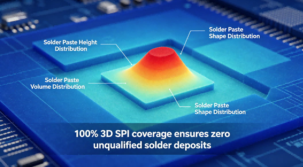
In-line 3D SPI (Solder Paste Inspection) to verify exact paste volume and registration accuracy down to 0201 footprints.
In-line 3D AOI (Automated Optical Inspection) for real-time tracking of component placement and solder wetting geometry.
Depth-controlled backdrilling capabilities to reliably eliminate via stubs on high-speed digital designs.
We focus on delivering transparent, predictable engineering data and rigorous process control to support our clients’ NPI cycles and serial production requirements.
1. What material is best for high-frequency board-level shielding cans?
Tin-plated steel is often preferred because it balances corrosion resistance with effective attenuation for both electric and magnetic fields at a reasonable cost. For weight-sensitive designs or harsh environments, nickel-silver is frequently chosen because it resists oxidation without requiring secondary plating.
2. How do shielding cans affect PCB thermal management?
Shielding cans trap heat generated by internal high-power components, such as power amplifiers or processors. To prevent thermal hotspots, designs should include thermal vias that route heat down to internal ground planes, or use perforated shields combined with pre-applied thermal interface materials (TIMs) that conduct heat directly to the shield casing.
3. How many ground stitching vias are needed around an EMI shielding can?
To maintain the integrity of the shield, grounding vias should be placed at pitch intervals equal to a fraction of the target signal’s wavelength—typically less than one-twentieth ($\lambda / 20$) of the highest operating frequency. Wider spacing can allow high-frequency harmonic energy to radiate through the gaps between vias.
4. Can an effective multi-layer PCB layout eliminate the need for external metal shielding cans?
For many digital designs operating under 1 GHz, an optimized layer stackup, careful zoning of noisy components, and proper filtering can often achieve EMC compliance without external cans. However, for high-power RF transmitters, sensitive radar front-ends, or ultra-low-noise medical analog lines, physical metal shielding remains standard practice to isolate the circuitry from ambient external fields.
Achieving reliable signal integrity and strict EMC compliance requires a production partner that understands how to translate layout specifications into robust, repeatable hardware. Contact the engineering team at Guangzhou Huachuang Precision Technology Co., Ltd. (HCJMPCBA) today to submit your Gerber files and bill of materials (BOM) for a comprehensive DFM review and competitive manufacturing quotation.
Guangzhou Huachuang Precision Technology Co., Ltd. is a leading PCBA manufacturer offering high-qual

A pcb board—also known as a printed circuit board—forms the backbone of modern electronics, link
Tired of PCBA failures? Nearly 60% of soldering issues begin at stencil printing. Learn how HCJMPCBA