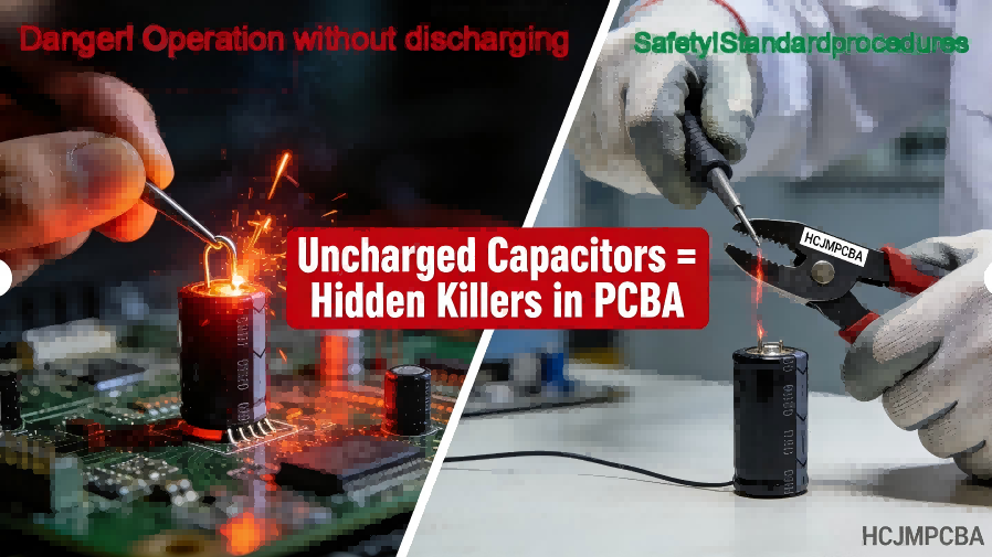
10 Compelling Reasons Why Discharging Capacitors Is Non-Negotiable + Expert’s Step-by-Step Guide on How to Discharge a Capacitor Safely
Discharging capacitors is a critical safety and quality control step in electronics and PCBA work. T
How to print pcb board files efficiently? Prototyping a custom board relies heavily on transferring digital layouts onto copper-clad laminates via heat, chemical stripping, or precise ablation. This comprehensive manufacturing guide is maintained by the HCJMPCBA engineering team and updated with production checklists. It provides the exact frameworks required to convert a laser printer circuit board concept into a reliable hardware asset.
Toner Density Dictates Yield: When printing pcb with laser printer systems for chemical masking, the solid ink density must be maximize-configured to block ferric chloride or ammonium persulfate etchants completely.
Thermal Stress is the Root of Defect: Manual heat press methods during DIY toner transfers introduce uneven Z-axis mechanical stress, often leading to hairline copper fractures that can only be diagnosed via advanced microscopy.
Scale Requires True Sublimation: While a laser etch circuit board approach bypasses hazardous wet chemical handling during initial engineering sprints, high-volume manufacturing demands automated pcb laser cutting and industrial laser pcb etching to achieve reproducible trace clearances.
| Engineering Target | DIY Laser Toner Transfer | Industrial Laser PCB Etching | Full-Scale Turnkey PCBA |
| Ideal Batch Size | $1 – 3$ units | $1 – 50$ units (Fast Prototyping) | $100 – 100,000+$ units (Mass Production) |
| Minimum Trace/Space | $\ge 0.5\text{mm}$ ($20\text{mil}$) | $\ge 0.1\text{mm}$ ($4\text{mil}$) | Down to $0.05\text{mm}$ / $0.05\text{mm}$ ($2\text{mil}$) |
| Substrate Compatibility | Standard FR-4 Only | FR-4, Rigid-Flex, Ceramic | Aluminum, HDI, Taconic, Teflon |
| Tooling Mechanism | Glossy paper + Household Iron | High-precision laser engraver pcb | CNC Masking + Multi-zone Reflow |
| Traceability Level | Manual labeling | laser etch pcb Serialization | Full Component Lot & Serial Mapping |
Laser Printing Microscopic Comparison Diagram
1. Gerber File Preparation and Mirror Configuration
Export your layout design files (Gerber RS-274X data package, including copper layers, solder mask, and NC drill datasets) from your EDA suite. When configuring the output for a printed circuit board laser printer, the top copper layer must be flipped or mirrored before printing. This ensures that when the toner face is pressed directly down onto the copper board, the orientation matches the intended schematic layout.
2. Substrate Degreasing and Surface Preparation
Select a high-quality, copper-clad laminate board compliant with the UL 796 safety standard. The copper surface must be completely free of oxidation, fingerprints, and oils. Use a fine abrasive pad (such as $1200$-grit sandpaper) to scrub the board under running water until the copper exhibits a uniform, bright pink coloration. Dry immediately with a lint-free cloth to prevent flash oxidation.
3. High-Density Toner Transfer via Laser Jet Systems
Feed a high-resolution, heavy glossy paper or magazine stock into a dedicated pcb laser printer. Adjust the print settings to disable all toner-saving profiles, set the resolution to maximum ($1200\text{DPI}$ or greater), and force the print mode to “Heavy Stock.” The resulting laser printer circuit board template must exhibit thick, shiny, Jet-Black lines with no visible paper showing through the solid copper ground planes.
4. Thermal Fusion and Toner Migration
Align the printed sheet face-down onto the prepared copper substrate. Introduce the assembly into a temperature-controlled laminator or apply steady pressure using a standard household iron preheated to approximately $180^\circ\text{C} – 200^\circ\text{C}$. Apply firm, isotropic mechanical pressure over the entire surface area for $3 – 5$ minutes. The heat forces the plastic polymers within the toner matrix to crosslink and fuse directly with the bare copper molecules.
5. Paper Peeling and Micro-Drying
Submerge the hot, laminated board into a bath of warm water mixed with a drop of mild detergent. Allow the paper backing to soak for $10 – 15$ minutes until it becomes completely saturated and translucent. Gently roll the paper pulp away using your thumb, taking care not to lift the fragile toner lines beneath. Inspect the board under a magnifying glass; any minor trace breaks must be manually repaired using an oil-based permanent marker.
6. Chemical Masking or Laser PCB Etching Ablation
For traditional DIY methods, submerge the board into an aqueous ferric chloride ($FeCl_3$) chemical solution. The uncovered copper will dissolve, leaving the toner-protected circuits intact. However, for industrial prototyping, engineers utilize a dedicated laser engraver pcb setup. Instead of masking with messy chemicals, a fine-tuned fiber laser beam directly burns away the unwanted copper areas according to the CAD coordinates, executing clean laser cutting pcb board profiles without modifying the core properties of the substrate.
7. Toner Stripping and Pre-Incircuit Clean
Once etching or laser ablation concludes, the hardened toner mask must be removed. Sponge the surface with pure acetone or rubbing alcohol. The plastic ink will readily dissolve, exposing pristine, shiny copper traces underneath. Wash the completed board with isopropyl alcohol (IPA) to eliminate organic chemical residues before moving to component mounting.
8. Via Drilling and Mechanical Routing
For through-hole configurations, mount the board onto a high-speed micro-drill press. Use solid carbide drill bits matching your Gerber NC drill parameters. For precision routing or cutting odd shapes out of the larger panel, a commercial-grade laser cutting pcb system provides much cleaner board edges than mechanical routers, eliminating the risk of delamination between the copper foil and the epoxy resin base.
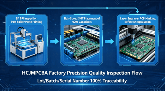
9. Final Inspection and Protective Conformal Solder Coating
The newly formed traces are highly susceptible to moisture and oxidation. Apply a thin layer of liquid solder mask or rosin flux coating. In automated facilities like HCJMPCBA, we run the populated board through a 3D SPI (Solder Paste Inspection) line and multi-zone reflow ovens to guarantee that every surface-mounted component bonds permanently with the copper traces.
To translate basic desktop concepts into field-ready assemblies, HCJMPCBA replaces manual, error-prone steps with structured verification criteria. Our factory engineering team deploys the following rigorous protocol for every mass production batch:
| Test Parameter | Standard Method Number & Revision | Sample Plan / AQL | Test Conditions | Raw Data Deliverables |
| Ionic Cleanliness | IPC-TM-650, Method 2.3.25, Rev C | Zero Defect Target ($C=0$) | Resistivity of Solvent Extract (ROSE) testing | $\mu\text{g}/\text{cm}^2$ NaCl equivalent charts |
| Thermal Shock | MIL-STD-202, Method 107, Rev G | $12$ Units per batch | $-40^\circ\text{C}$ to $+125^\circ\text{C}$, $100$ continuous cycles | Cross-sectional micro-imaging logs |
| Solderability | IPC-J-STD-002, Rev E | Visual Inspection AQL 0.4 | Wetting balance test at $245^\circ\text{C}$ solder pot | Force-time wetting curves |
| Impedance Continuity | IPC-2141B / IEC 61188-5-1 | 100% of Coaxial/RF Traces | TDR (Time Domain Reflectometry) at $10\text{GHz}$ | Real-time Ohm differential data plots |
| Trace Attachment | IPC-TM-650, Method 2.4.9, Rev E | 3 Panels per Lot | Peel strength analysis of copper to laminate | Newton per millimeter (N/mm) log sheets |
Industrial Grade Pcba Traceability And Inspection Link Diagram
Global procurement professionals and OEM engineers may copy, paste, and modify the following text block directly into their Request for Quotes (RFQs) or Statement of Work (SOW) documents to ensure all candidate vendors maintain automotive-grade tracking and production standards:
“The supplier must ensure 100% product accountability by etching a persistent barcode on the non-functional edge of each PCB board via an industrial laser etch pcb process. All manufacturing steps, component sourcing, and electrical validations must be backed by transparent traceability records linked down to the individual serial number level. No manual chemical-toner masking methods are permitted for batches exceeding 50 units. The vendor is required to supply raw testing data files for IPC-A-610 Class 3 compliance along with the certificate of conformance upon shipment.”
Using Standard Copy Paper: Using standard copy paper instead of clay-coated glossy photo paper prevents the toner from detaching properly, leading to torn, incomplete traces after the water bath.
Ignoring Copper Board Oxide Films: Forgetting to polish the micro-thin layer of copper oxide off the bare board before thermal lamination prevents the melted toner from bonding tightly, which causes the layout to peel away during subsequent wet chemical etching steps.
Improper Temperature Calibration: Running the heat transfer process below $150^\circ\text{C}$ leads to cold, brittle toner that flakes off easily. Conversely, exceeding $220^\circ\text{C}$ liquefies the toner excessively, broadening your trace profiles and creating devastating bridging short circuits between tightly spaced pins.
Neglecting Mechanical Stress Points: Cutting rigid multi-layer laminates with manual tin snips creates massive micro-fractures inside the internal fiberglass grid. This eventually results in intermittent circuit dropouts under vibration, a defect easily eliminated by upgrading to automated pcb laser cutting.
Lack of Production Traceability: Making dozens of identical boards without an integrated tracking code makes tracking down systemic errors impossible. True hardware scalability requires an automated laser engraver pcb system to engrave distinct serial numbers on every unit.
Consider a field development company developing a smart telemetry system for high-vibration off-road vehicles. During Phase 1, the design engineer successfully learns how to make a board using a standard desktop office printer to create a quick proof-of-concept module. It functions fine on the lab bench.
However, during Phase 2 (Field Trial Deployment), the team needs $500$ fully built modules to install into field units. Attempting to manually print, iron, wash, etch, drill, and hand-solder hundreds of boards introduces massive variations in trace thickness and cold solder joints. At this critical junction, the engineering firm hands the design files over to an experienced contract assembly house like HCJMPCBA. By utilizing professional automated lines, optical inspections, and ruggedized conformal coatings, the design transitions smoothly into a scalable, field-hardened product.
Q1: Why is an industrial laser etch circuit board more reliable than home-brewed chemical etching?
Manual chemical etching depends heavily on fluid dynamics, bath temperatures, and timing, which can lead to uneven undercut profiles along trace edges. Conversely, industrial automated lasers ablate copper with micron-level precision, preserving straight sidewalls and consistent impedance matching across high-speed signal paths.
Q2: Can a standard office laser printer print directly onto a copper board?
No, standard office printers cannot handle rigid copper-clad substrates because their mechanical rollers require flexible paper sheets. To bypass paper transfer stages entirely, manufacturing facilities utilize specialized industrial flatbed printed circuit board laser printer machines designed to track across flat surfaces.
Q3: How does pcb laser cutting protect thin, multi-layer rigid-flex board stacks?
Traditional mechanical shear matrices push down on board edges, causing shear stress that can delaminate outer copper layers. Advanced laser cutting pcb systems vaporize the substrate material instantly with narrow beam paths, leaving clean edges completely free of structural fractures or delamination risks.
Q4: What exact trace density can HCJMPCBA handle for industrial-grade turnkey orders?
Our high-speed automated production floor easily accommodates dense layouts featuring 0201 or 01005 component packages, ultra-fine pitch BGAs, and advanced QFN profiles. Every batch is verified by 3D SPI and automated X-ray analysis to maintain field defect rates below industry standards.
Q5: How do you enforce component batch traceability down to the individual serial number?
Every panel arriving on our line is marked with a permanent tracking code via an industrial laser engraver pcb system. Our active ERP system logs the specific raw material batch, the component feeder lot numbers, and the automated reflow temperature profile, binding all data directly to that unique serial identifier.
When partner companies transition their products to our facility, we reduce procurement anxiety by offering transparent manufacturing data logs:
DFM Compliance Report: Full engineering analysis highlighting potential trace layout risks before we start production.
Solder Paste Height Maps: Automated raw data records from our 3D SPI system showing consistent print volume across every fine-pitch pad.
X-Ray Laminography Files: Internal structural imagery validating perfect ball wetting and void-free connections beneath multi-layer BGA components.
AQL Inspection Summaries: Detailed lot-by-lot quality yields based on your preferred internal acceptance sampling plans.
For more information about PCBA services, please contact Guangzhou Huachuang Precision Technology(HCJMPCBA).
Update triggers: standard revision changes / recurring questions / production checklist updates.
Disclaimer: All cited technical standards (IPC, IEC, JEDEC, UL) are property of their respective regulatory organizations and are utilized herein strictly to define high-reliability electronic product manufacturing parameters.
Discharging capacitors is a critical safety and quality control step in electronics and PCBA work. T

Discover what is an ICT tester and how in-circuit testing (ICT) ensures PCB/PCBA quality with fast,
This article provides an in-depth exploration of PCBA technology, its evolution, key processes, chal